- 您现在的位置:买卖IC网 > PDF目录69003 > L6563STR (STMICROELECTRONICS) POWER FACTOR CONTROLLER, PDSO14 PDF资料下载
参数资料
| 型号: | L6563STR |
| 厂商: | STMICROELECTRONICS |
| 元件分类: | 稳压器 |
| 英文描述: | POWER FACTOR CONTROLLER, PDSO14 |
| 封装: | ROHS COMPLIANT, SOP-14 |
| 文件页数: | 25/42页 |
| 文件大小: | 1230K |
| 代理商: | L6563STR |
第1页第2页第3页第4页第5页第6页第7页第8页第9页第10页第11页第12页第13页第14页第15页第16页第17页第18页第19页第20页第21页第22页第23页第24页当前第25页第26页第27页第28页第29页第30页第31页第32页第33页第34页第35页第36页第37页第38页第39页第40页第41页第42页
L6563S
Application information
Doc ID 16116 Rev 3
31/42
6.7
Power management/housekeeping functions
A special feature of this IC is that it facilitates the implementation of the “housekeeping”
circuitry needed to co-ordinate the operation of the PFC stage to that of the cascaded DC-
DC converter. The functions realized by the housekeeping circuitry ensure that transient
conditions like power-up or power down sequencing or failures of either power stage be
properly handled.
This device provides some pins to do that. One communication line between the IC and the
PWM controller of the cascaded dc-dc converter is the pin PWM_LATCH (Figure 44b),
which is normally open (high impedance) when the PFC works properly, and goes high if it
loses control of the output voltage (because of a feedback loop disconnection) with the aim
of latching off the PWM controller of the cascaded dc-dc converter as well (see “Feedback
failure protection” section for more details).
A second communication line can be established via the disable function included in the
PFC_OK pin (see “Feedback failure protection” section for more details). Typically this line is
used to allow the PWM controller of the cascaded dc-dc converter to drive in burst mode
operation the L6563S in case of light load and to minimize the no-load input consumption.
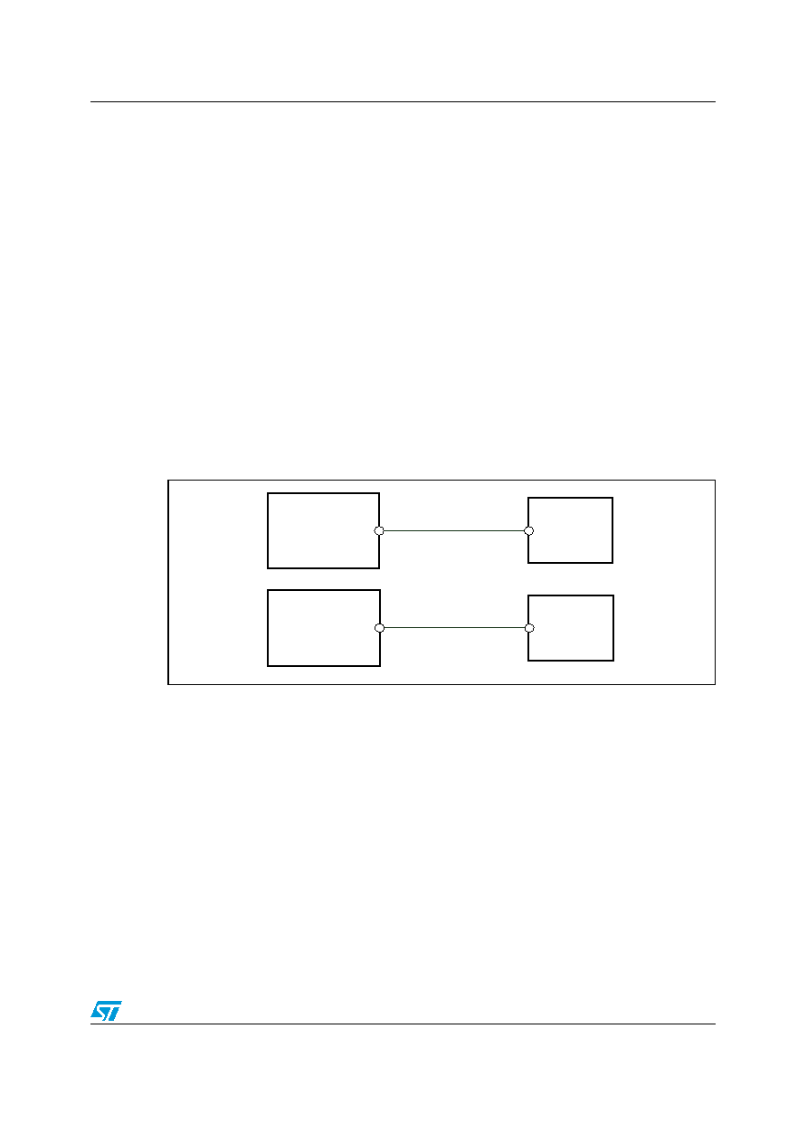
Interface circuits like those are shown in Figure 43.
Figure 43.
Interface circuits that let dc-dc converter's controller IC drive L6563S in
burst mode
The third communication line is the pin PWM_STOP (#9), which works in conjunction with
the pin RUN (#10). The purpose of the PWM_STOP pin is to inhibit the PWM activity of both
the PFC stage and the cascaded dc-dc converter. The pin is an open collector, normally
open, that goes low if the device is disabled by a voltage lower than 0.8 V on the RUN pin. It
is important to point out that this function works correctly in systems where the PFC stage is
the master and the cascaded dc-dc converter is the slave or, in other words, where the PFC
stage starts first, powers both controllers and enables/disables the operation of the dc-dc
stage. The pin RUN can be used to start and stop the main converter. In the simplest case,
to enable/disable the PWM controller the pin PWM_STOP can be connected to the output of
the error amplifier (Figure 44a).
相关PDF资料 |
PDF描述 |
|---|---|
| L6563S | POWER FACTOR CONTROLLER, PDSO14 |
| L6564DTR | SWITCHING CONTROLLER, PDSO10 |
| L6564D | SWITCHING CONTROLLER, PDSO10 |
| L6585DE | POWER FACTOR CONTROLLER, PDSO20 |
| L6585DETR | POWER FACTOR CONTROLLER, PDSO20 |
相关代理商/技术参数 |
参数描述 |
|---|---|
| L6563TR | 功能描述:功率因数校正 IC POWER SUPPLY RoHS:否 制造商:Fairchild Semiconductor 开关频率:300 KHz 最大功率耗散: 最大工作温度:+ 125 C 安装风格:SMD/SMT 封装 / 箱体:SOIC-8 封装:Reel |
| L6564 | 制造商:STMICROELECTRONICS 制造商全称:STMicroelectronics 功能描述:10 pin transition-mode PFC controller |
| L6564D | 功能描述:IC PFC CTRLR TRANSITION 10SSOP RoHS:是 类别:集成电路 (IC) >> PMIC - PFC(功率因数修正) 系列:- 产品培训模块:GreenChip Synchronous Rectification Control Family of ICs 标准包装:1 系列:- 模式:间歇导电(DCM) 频率 - 开关:- 电流 - 启动:- 电源电压:8.6 V ~ 38 V 工作温度:-20°C ~ 150°C 安装类型:表面贴装 封装/外壳:14-SOIC(0.154",3.90mm 宽) 供应商设备封装:14-SO 包装:Digi-Reel® 其它名称:568-5348-6 |
| L6564DTR | 功能描述:功率因数校正 IC Transition Mode PFC 5mA 90uA 1.5% Ref RoHS:否 制造商:Fairchild Semiconductor 开关频率:300 KHz 最大功率耗散: 最大工作温度:+ 125 C 安装风格:SMD/SMT 封装 / 箱体:SOIC-8 封装:Reel |
| L6564H | 功能描述:功率因数校正 IC High Voltage Startup Trans-Mode PFC 700V RoHS:否 制造商:Fairchild Semiconductor 开关频率:300 KHz 最大功率耗散: 最大工作温度:+ 125 C 安装风格:SMD/SMT 封装 / 箱体:SOIC-8 封装:Reel |
发布紧急采购,3分钟左右您将得到回复。