- 您现在的位置:买卖IC网 > PDF目录97995 > L6615N (STMICROELECTRONICS) 1-CHANNEL POWER SUPPLY SUPPORT CKT, PDIP8 PDF资料下载
参数资料
| 型号: | L6615N |
| 厂商: | STMICROELECTRONICS |
| 元件分类: | 电源管理 |
| 英文描述: | 1-CHANNEL POWER SUPPLY SUPPORT CKT, PDIP8 |
| 封装: | MINI, DIP-8 |
| 文件页数: | 4/20页 |
| 文件大小: | 394K |
| 代理商: | L6615N |
L6615
12/20
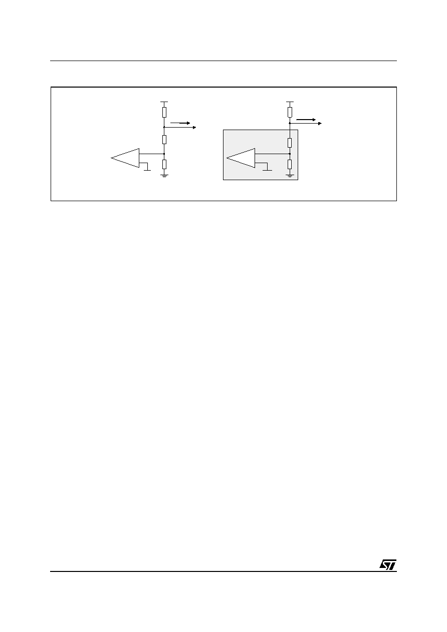
Figure 12. ADJ network
To set the RADJ value it is necessary to know the tolerance required of the power supply output voltage
(VOUT±VO); the maximum difference between master and slave output voltage is 2*VO and this amount
represents the voltage that the L6615 must be able to correct.
Now two different approaches are feasible depending on whether the SMPS (whose output current must
be shared) has to be completely designed or it is an "off the shelf" component and only the current sharing
section must be designed.
In the first case, the adjustment resistor (RADJ) can be considered as a fraction of the high resistor of the
feedback divider RH (see fig.12.a): typically the first step consist of fixing the current flowing, under steady
state condition, through the feedback divider IFB; by choosing the value for R2:
we will have:
It can be an useful rule of thumb to use RADJ lower than (or equal to) one tenth of R1, considering that, in
worst case condition, it will be:
This value must not exceed the one indicated in the "Electrical characteristic section" but this is very easy
to meet, as one can easily see by using sensible values for
VOUT and R2.
In the second case (fig 12.b), the feedback divider has been already designed by the SMPS manufacturer
and it is not possible to modify it: the design of RADJ must be done to make the L6615 able to correct the
maximum spread without significantly shifting the SMPS regulation point. A minimum RADJ value can be
found by:
where IADJ(max) is 8mA.
Especially for low voltage output buses it is important to avoid adjustment network saturation; the design
must satisfy the following relationship:
where VADJ(MIN) can be found in the "Electrical characteristic section" for different IADJ values.
V
OUT
V
REF
Off the shelf
POWER SUPPLY
R
ADJ
E/A
to L6615
ADJ pin
I
ADJ
V
OUT
V
REF
R
ADJ
E/A
to L6615
ADJ pin
I
ADJ
R
1
R
2
a)
b)
V
OUT
V
REF
Off the shelf
POWER SUPPLY
R
ADJ
E/A
to L6615
ADJ pin
I
ADJ
V
OUT
V
REF
R
ADJ
E/A
to L6615
ADJ pin
I
ADJ
R
1
R
2
a)
b)
I
FB
V
REF
R
2
--------------
=
R
H
R
1
R
ADJ
+
V
OUT
V
REF
---------------
1
–
R
2
==
I
ADJ max
()
V
OUT
R
ADJ
------------------
=
R
ADJ min
()
V
OUT
I
ADJ ma x
()
--------------------------
=
V
OUT
R
ADJ
I
ADJ
I
FB
+
() V
ADJ MIN
()
>
–
相关PDF资料 |
PDF描述 |
|---|---|
| L6711TR | 2 A SWITCHING CONTROLLER, 178 kHz SWITCHING FREQ-MAX, PQFP48 |
| L6711 | 2 A SWITCHING CONTROLLER, 178 kHz SWITCHING FREQ-MAX, PQFP48 |
| L6714TR | SWITCHING CONTROLLER, 170 kHz SWITCHING FREQ-MAX, PQFP64 |
| L6714 | SWITCHING CONTROLLER, 170 kHz SWITCHING FREQ-MAX, PQFP64 |
| L6725TR | 20 A SWITCHING CONTROLLER, 500 kHz SWITCHING FREQ-MAX, PDSO16 |
相关代理商/技术参数 |
参数描述 |
|---|---|
| L6622-01 | 制造商:HAMAMATSU 制造商全称:Hamamatsu Corporation 功能描述:130 KV MICROFOCUS X-RAY SOURCE |
| L-663 | 制造商:RHOMBUS-IND 制造商全称:Rhombus Industries Inc. 功能描述:CURRENT SENSE INDUCTOR |
| L6-6330 | 制造商: 功能描述: 制造商:undefined 功能描述: |
| L6660 | 制造商:STMICROELECTRONICS 制造商全称:STMicroelectronics 功能描述:MILLI-ACTUATOR DRIVER |
| L6668 | 功能描述:电流型 PWM 控制器 SMART PRIMARY CONTROLLER RoHS:否 制造商:Texas Instruments 开关频率:27 KHz 上升时间: 下降时间: 工作电源电压:6 V to 15 V 工作电源电流:1.5 mA 输出端数量:1 最大工作温度:+ 105 C 安装风格:SMD/SMT 封装 / 箱体:TSSOP-14 |
发布紧急采购,3分钟左右您将得到回复。