- 您现在的位置:买卖IC网 > PDF目录97995 > L6728D (STMICROELECTRONICS) 30 A SWITCHING CONTROLLER, 300 kHz SWITCHING FREQ-MAX, PDSO10 PDF资料下载
参数资料
| 型号: | L6728D |
| 厂商: | STMICROELECTRONICS |
| 元件分类: | 稳压器 |
| 英文描述: | 30 A SWITCHING CONTROLLER, 300 kHz SWITCHING FREQ-MAX, PDSO10 |
| 封装: | 3 X 3 MM, ROHS COMPLIANT, DFN-10 |
| 文件页数: | 29/33页 |
| 文件大小: | 1215K |
| 代理商: | L6728D |
第1页第2页第3页第4页第5页第6页第7页第8页第9页第10页第11页第12页第13页第14页第15页第16页第17页第18页第19页第20页第21页第22页第23页第24页第25页第26页第27页第28页当前第29页第30页第31页第32页第33页
L6728D
Pin description and connection diagram
Doc ID 16498 Rev 1
5/33
2
Pin description and connection diagram
2.1
Pin descriptions
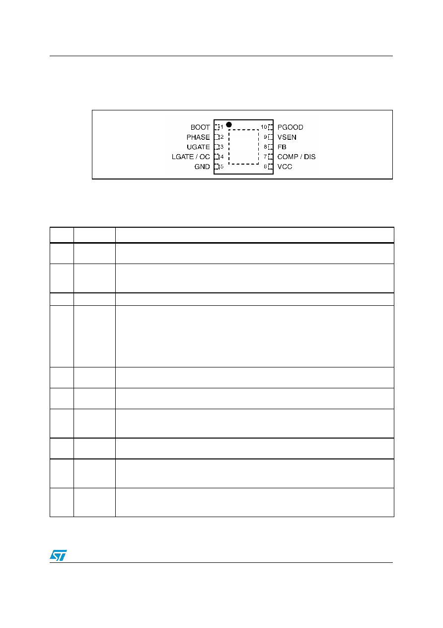
Figure 3.
Pin connection (top view)
L6728D
Table 2.
Pins description
Pin n°
Name
Function
1BOOT
HS driver supply. Connect through a capacitor (100 nF) to the floating node (LS-Drain) pin
and provide necessary bootstrap diode from VCC.
2
PHASE
HS driver return path, current-reading and adaptive-dead-time monitor. Connect to the LS
drain to sense
RDS(on) drop to measure the output current. This pin is also used by the
adaptive-dead-time control circuitry to monitor when HS MOSFET is OFF.
3
UGATE
HS driver output. Connect directly to HS MOSFET gate.
4
LGATE / OC
LGATE: LS driver output. Connect directly to LS MOSFET gate. OC: Overcurrent threshold
set. During a short period of time following VCC rising over the UVLO threshold, a 10
μA
current is sourced from this pin. Connect to GND with an ROCSET resistor greater than 5 kΩ to
program the OC threshold. The resulting voltage at this pin is sampled and held internally as
the OC set point. The maximum programmable OC threshold is 0.55 V. A voltage greater than
0.6 V activates an internal clamp and causes the OC threshold to be set at the maximum
value.
5GND
All internal references, logic and drivers are connected to this pin. Connect to the PCB ground
plane.
6VCC
Device and driver power supply. Operating range from 5 V to 12 V. Filter with at least 1 F
MLCC to GND.
7
COMP / DIS
COMP: Error amplifier output. Connect with an RF - CF // CP to FB to compensate the device
control loop. DIS: The device can be disabled by pushing this pin lower than 0.75 V (typ). By
setting the pin free, the device is enabled again.
8FB
Error amplifier inverting input. Connect with a resistor RFB to the output regulated voltage. An
output resistor divider may be used to regulate voltages higher than the reference.
9
VSEN
Regulated voltage sense pin for OVP and UVP protection and PGOOD. Connect to the output
regulated voltage, or to the output resistor divider if the regulated voltage is higher than the
reference.
10
PGOOD
Open drain output set free after SS has finished and pulled low when VSEN is outside the
relative window. Pull up to a voltage equal or lower than VCC. If not used it can be left
floating.
相关PDF资料 |
PDF描述 |
|---|---|
| L6911C | 1.3 A SWITCHING CONTROLLER, 1000 kHz SWITCHING FREQ-MAX, PDSO20 |
| L6911DTR | 1.3 A SWITCHING CONTROLLER, 1000 kHz SWITCHING FREQ-MAX, PDSO20 |
| L6911E | 1.3 A SWITCHING CONTROLLER, 1000 kHz SWITCHING FREQ-MAX, PDSO20 |
| L6911ETR | 1.3 A SWITCHING CONTROLLER, 1000 kHz SWITCHING FREQ-MAX, PDSO20 |
| L6924U013 | POWER SUPPLY SUPPORT CKT, PQCC16 |
相关代理商/技术参数 |
参数描述 |
|---|---|
| L6728DTR | 功能描述:电流型 PWM 控制器 Single-Phase PWM 5V to 12V Controller RoHS:否 制造商:Texas Instruments 开关频率:27 KHz 上升时间: 下降时间: 工作电源电压:6 V to 15 V 工作电源电流:1.5 mA 输出端数量:1 最大工作温度:+ 105 C 安装风格:SMD/SMT 封装 / 箱体:TSSOP-14 |
| L6728H | 功能描述:电压模式 PWM 控制器 Sgl Output 300 KHz DFN-10 RoHS:否 制造商:Texas Instruments 输出端数量:1 拓扑结构:Buck 输出电压:34 V 输出电流: 开关频率: 工作电源电压:4.5 V to 5.5 V 电源电流:600 uA 最大工作温度:+ 125 C 最小工作温度:- 40 C 封装 / 箱体:WSON-8 封装:Reel |
| L6728HTR | 功能描述:电流型 PWM 控制器 SINGLE PHASE PWM CNTRL PWR GOOD RoHS:否 制造商:Texas Instruments 开关频率:27 KHz 上升时间: 下降时间: 工作电源电压:6 V to 15 V 工作电源电流:1.5 mA 输出端数量:1 最大工作温度:+ 105 C 安装风格:SMD/SMT 封装 / 箱体:TSSOP-14 |
| L6728TR | 功能描述:DC/DC 开关控制器 Sngl phase PWM controller RoHS:否 制造商:Texas Instruments 输入电压:6 V to 100 V 开关频率: 输出电压:1.215 V to 80 V 输出电流:3.5 A 输出端数量:1 最大工作温度:+ 125 C 安装风格: 封装 / 箱体:CPAK |
| L6730 | 功能描述:DC/DC 开关控制器 Adjustable Step Down Controller RoHS:否 制造商:Texas Instruments 输入电压:6 V to 100 V 开关频率: 输出电压:1.215 V to 80 V 输出电流:3.5 A 输出端数量:1 最大工作温度:+ 125 C 安装风格: 封装 / 箱体:CPAK |
发布紧急采购,3分钟左右您将得到回复。