- 您现在的位置:买卖IC网 > PDF目录30713 > L9942XP1TR (STMICROELECTRONICS) STEPPER MOTOR CONTROLLER, 2.5 A, PDSO24 PDF资料下载
参数资料
| 型号: | L9942XP1TR |
| 厂商: | STMICROELECTRONICS |
| 元件分类: | 运动控制电子 |
| 英文描述: | STEPPER MOTOR CONTROLLER, 2.5 A, PDSO24 |
| 封装: | ROHS COMPLIANT, SSOP-24 |
| 文件页数: | 15/40页 |
| 文件大小: | 639K |
| 代理商: | L9942XP1TR |
第1页第2页第3页第4页第5页第6页第7页第8页第9页第10页第11页第12页第13页第14页当前第15页第16页第17页第18页第19页第20页第21页第22页第23页第24页第25页第26页第27页第28页第29页第30页第31页第32页第33页第34页第35页第36页第37页第38页第39页第40页
Functional description of the logic with SPI
L9942
Doc ID 11778 Rev 6
Note:
Due to this safety functionality a daisy chaining of SPI is not possible. Instead, a parallel
operation of the SPI bus by controlling the CSN signal of the connected ICs is
recommended.
4.6
Serial data out (DO)
The data output driver is activated by a logical low level at the CSN input and will go from
high impedance to a low or high level depending on the status bit 0 (fault condition). The first
rising edge of the CLK input after a high to low transition of the CSN pin will transfer the
content of the selected status register into the data out shift register. Each subsequent
falling edge of the CLK will shift the next bit out.
4.7
Serial clock (CLK)
The CLK input is used to synchronize the input and output serial bit streams. The data input
(DI) is sampled at the rising edge of the CLK and the data output (DO) will change with the
falling edge of the CLK signal.
4.8
Data register
The device has eight data registers. The first three bits (bit 0 ... bit 2) at the DI-input are used
to select one of the input registers. All bits are first shifted into an input shift register. After
the rising edge of CSN the contents of the input shift register will be written to the selected
Input Data Register only if a frame of exact 16 data bits are detected. The selected register
will be transferred to DO during the current communication frame.
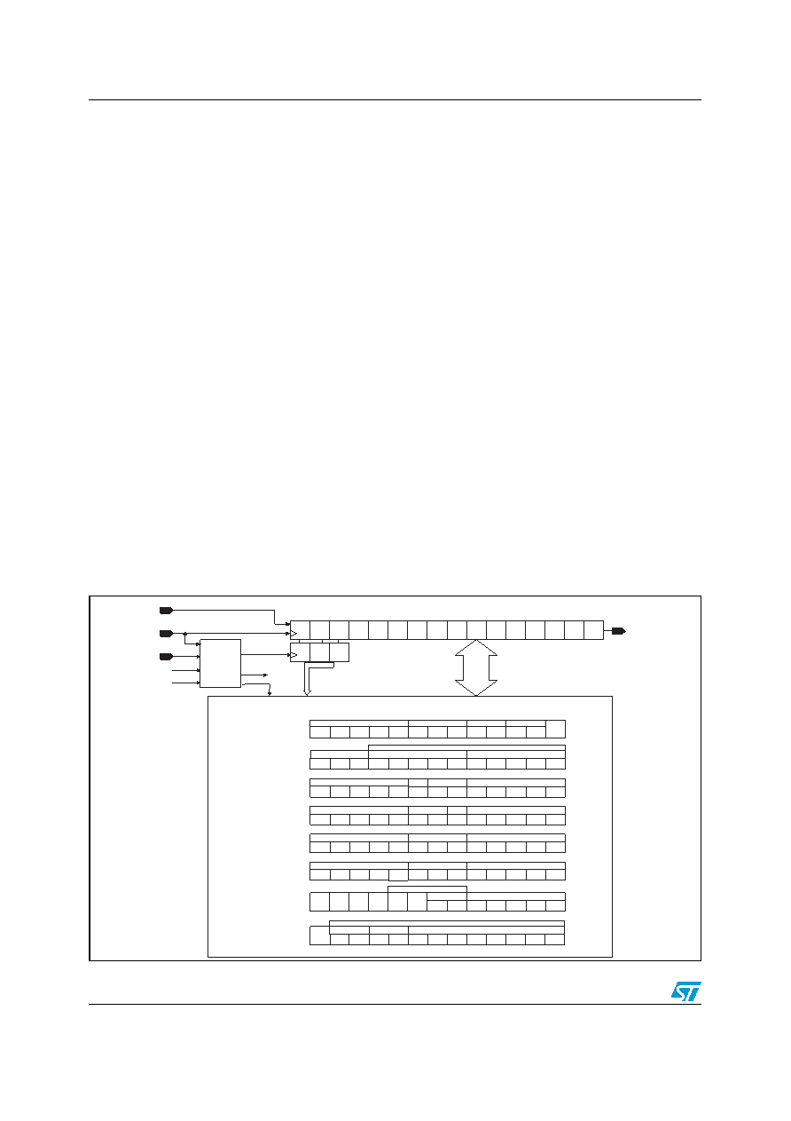
Figure 9.
SPI and registers
D
DI
CLK_ADR
D1
A1
D0
A2
D3
D4
D5
D6
D7
D8
D9
D10
D11
DO
DIR
Register 0
AI0
AI1
AI2
AI3
AI4
BI0
BI1
BI2
BI3
BI4
DAC Phase B
DAC Phase A
Register 2
P0
P1
P2
P3
P4
Phase
A
Phase
B
Register 7
D2
D12
Phase Counter
Register 1
I0
I1
I2
I3
I4
I0
I1
I2
I3
I4
Current Profile 0
Current Profile 1
OVW
OV
Openload
LSA1
HSA1
LSA2
HSA2
LSB1
LSB2
HSB1
HSB2
Overcurrent
UV
OV(W)
CSN
CLK
INT_2MHz
SPI-
Controll
POR
Slew Rate
Step Mode
SR0
SR1
ST1
ST0
DAC_Scale
DC1
DC2
Temperature
VS Monitor
SEL_ERROR
SPI2REG
D
A1
A0
A2
TSD
TW
RREF
Error
CLR7
CLR6
Read-Only
DC0
Read Only
PWM
Freq
FT
I0
I1
I2
I3
I4
Current Profile 8
Read-Only
ST
I0
I1
I2
I3
I4
I0
I1
I2
I3
I4
Current Profile 2
Current Profile 3
NPWM
D0
D1
PWM Counter
I0
I1
I2
I3
I4
I0
I1
I2
I3
I4
Current Profile 4
Current Profile 5
I0
I1
I2
I3
I4
I0
I1
I2
I3
I4
Current Profile 6
Current Profile 7
Decay Mode
DM0
DM1
DM2
SST
A0
Test only
PWM
PWM Counter
D5
D6
D7
D2
D3
D4
T0
T1
Register 3
Register 4
Register 5
Register 6
相关PDF资料 |
PDF描述 |
|---|---|
| L9949TR | BRUSH DC MOTOR CONTROLLER, 10 A, PDSO20 |
| L9950XPTR | BRUSH DC MOTOR CONTROLLER, 10 A, PDSO36 |
| L9950 | BRUSH DC MOTOR CONTROLLER, 10 A, PDSO36 |
| L9950TR | BRUSH DC MOTOR CONTROLLER, 10 A, PDSO36 |
| L9953XPTR | BRUSH DC MOTOR CONTROLLER, 10 A, PDSO36 |
相关代理商/技术参数 |
参数描述 |
|---|---|
| L9946 | 制造商:未知厂家 制造商全称:未知厂家 功能描述:DC Motor Controller/Driver |
| L9947 | 制造商:STMICROELECTRONICS 制造商全称:STMicroelectronics 功能描述:QUAD HALF-BRIDGE AND SINGLE HIGH-SIDE DRIVER |
| L9947L | 制造商:STMicroelectronics 功能描述: |
| L9947S | 功能描述:马达/运动/点火控制器和驱动器 Quad Half Bridge RoHS:否 制造商:STMicroelectronics 产品:Stepper Motor Controllers / Drivers 类型:2 Phase Stepper Motor Driver 工作电源电压:8 V to 45 V 电源电流:0.5 mA 工作温度:- 25 C to + 125 C 安装风格:SMD/SMT 封装 / 箱体:HTSSOP-28 封装:Tube |
| L9949 | 功能描述:功率驱动器IC Door Actuator RoHS:否 制造商:Micrel 产品:MOSFET Gate Drivers 类型:Low Cost High or Low Side MOSFET Driver 上升时间: 下降时间: 电源电压-最大:30 V 电源电压-最小:2.75 V 电源电流: 最大功率耗散: 最大工作温度:+ 85 C 安装风格:SMD/SMT 封装 / 箱体:SOIC-8 封装:Tube |
发布紧急采购,3分钟左右您将得到回复。