- 您现在的位置:买卖IC网 > PDF目录43902 > LB11820M BRUSHLESS DC MOTOR CONTROLLER, 0.04 A, PDSO30 PDF资料下载
参数资料
| 型号: | LB11820M |
| 元件分类: | 运动控制电子 |
| 英文描述: | BRUSHLESS DC MOTOR CONTROLLER, 0.04 A, PDSO30 |
| 封装: | 0.375 INCH, MFP-30 |
| 文件页数: | 7/17页 |
| 文件大小: | 484K |
| 代理商: | LB11820M |
No. 7104-15/17
LB11820M
6. Drive Method
The output duty can be controlled according to any of following methods.
Control with the VCTL pin voltage
For the control voltage, refer to the electric characteristics. For control with the VCTL pin, set the PWMIN pin voltage
to the L level.
Control with the voltage applied to the TOC pin
The TOC pin voltage and PWM oscillation waveform are compared to determine the output duty. The output duty
becomes 0 % when the TOC pin voltage exceeds VOH (PWM) (3.0 V typ) and 100% when it becomes lower than the
VOL (PWM) (1.2 V typ). For control with the TOC pin, set the PWMIN pin voltage to the L level.
For control with the input level other than the internal CTL amp control input level, external connection of amp allows
setting to the arbitrary input level (with the external amp output connected to the TOC pin). For control from the TOC
pin, fix the VCTL pin voltage.
For an application in which the regulated voltage is applied to the TOC pin through resistor division, etc., it is
necessary to take into account the effect of resistor (about 20 k
) incorporated between the TOC pin and CTL amp
output. (Variation about ±20%, temperature characteristics about +0.3%/°C). If the noise is included in the voltage to
be applied to the TOC pin, chattering may occur in the output. In this case, stabilization with a capacitor is necessary.
Pulse control with the PWMIN pin
The output can be controlled on the basis of duty obtained by entering the pulse in the PWMIN pin. The output can be
turned ON when the L-level input voltage is applied to the PWM pin and OFF when the H-level input voltage is
applied. With the PWMIN pin open, the output becomes the H level and is turned OFF. If input with reversed logic is
necessary, addition of external Tr (NPN) may be enough.
For control with the PWMIN pin, set the VCTL pin voltage that is more than the VCTL2 voltage (output duty set to
100%) or connect the TOC pin to GND.
7. Hall Input Signal
The Hall input requires the signal input with an amplitude exceeding the hysteresis width (50 mV max). Considering
the effect of noise and phase displacement, the input with the amplitude of 120 mV or more is recommended.
When the noise causes disturbance in the output waveform (at a time of phase change) or HP output (Hall signal three-
phase synthesis output), insert a capacitor to the input to prevent such trouble. The Hall input is used as a signal to
determine the input to the restriction protection circuit and the protection circuit during reverse. Though noise is
ignored to a certain degree, due attention must be paid when using these protection circuits.
When all three phases of Hall input signal are entered, the output is turned OFF entirely (all of UL, VL, WL, UH, VH,
and WH OFF).
To enter the Hall IC output, fix one side of input (+ or –) to the voltage within the common-mode input range for Hall
device. This will allow input from 0 to VCC1 for another single-side input.
8. Circuit for Low-Voltage Protection
This circuit detects the voltage applied to the LVS pin. When this voltage drops below the operation voltage (see the
electric characteristics), the one-side output (UH, VH, and WH) is turned OFF. To prevent repetition of output ON/OFF
near the protection activation voltage, the hysteresis is provided. Accordingly, the output is not recovered unless the
voltage rises by about 0.5 V above the activation voltage.
The protection activation voltage is for the 5 V system detection level. The detection level can be raised by connecting
the zenor diode in series to the LVS pin and by shifting the detection level. The LVS pin inrush current at a time of
detection is about 65 A. To stabilize rise of the zenor diode voltage, increase the diode current by inserting the
resistor between the LVS pin and GND.
When the protection circuit is not used, apply a voltage on a level where the protection is not activated, instead of
setting the LVS pin open (output OFF with the pin open).
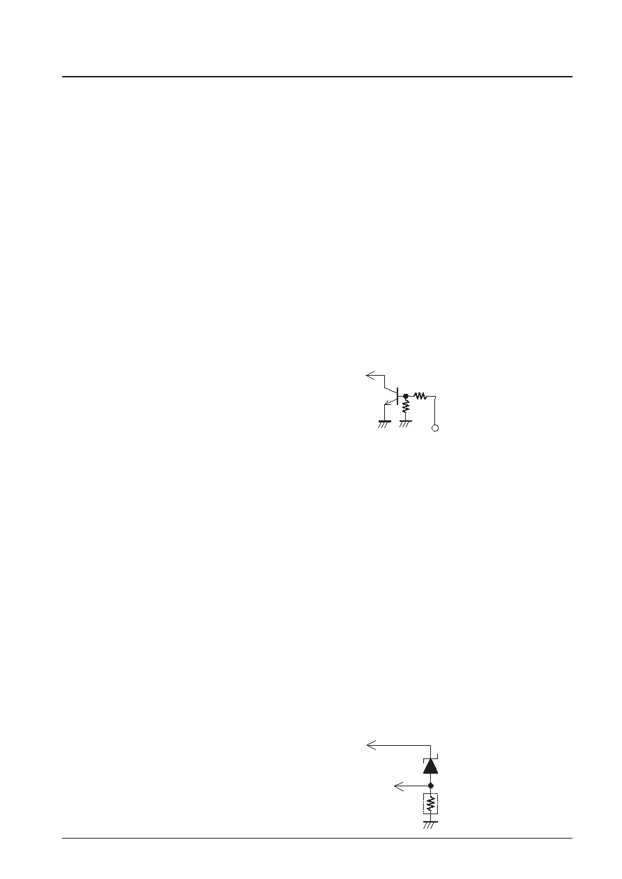
To pin PWMIN
Pulse input
To detection power supply
To pin LVS
相关PDF资料 |
PDF描述 |
|---|---|
| LB11822 | BRUSHLESS DC MOTOR CONTROLLER, 3.1 A, DFM28 |
| LB11823M | BRUSHLESS DC MOTOR CONTROLLER, 0.04 A, PDSO36 |
| LB11847 | STEPPER MOTOR CONTROLLER, 1.75 A, PDIP28 |
| LB11868V | DISK DRIVE MOTOR CONTROLLER, PDSO20 |
| LB11870 | BRUSHLESS DC MOTOR CONTROLLER, 1.8 A, PDSO48 |
相关代理商/技术参数 |
参数描述 |
|---|---|
| LB11822 | 制造商:未知厂家 制造商全称:未知厂家 功能描述: |
| LB11822-E | 功能描述:马达/运动/点火控制器和驱动器 RoHS:否 制造商:STMicroelectronics 产品:Stepper Motor Controllers / Drivers 类型:2 Phase Stepper Motor Driver 工作电源电压:8 V to 45 V 电源电流:0.5 mA 工作温度:- 25 C to + 125 C 安装风格:SMD/SMT 封装 / 箱体:HTSSOP-28 封装:Tube |
| LB11823M | 制造商:SANYO 制造商全称:Sanyo Semicon Device 功能描述:Direct PWM Drive Brushless Motor Predriver for OA Products |
| LB11823M(36SOP) | 制造商:未知厂家 制造商全称:未知厂家 功能描述:Controller Miscellaneous - Datasheet Reference |
| LB11824 | 制造商:SANYO 制造商全称:Sanyo Semicon Device 功能描述:Direct PWM Drive Brushless Motor Predriver for On-Demand Water Heater and Air Conditioner Motors |
发布紧急采购,3分钟左右您将得到回复。