- 您现在的位置:买卖IC网 > PDF目录30736 > LC78648E SPECIALTY CONSUMER CIRCUIT, PQFP80 PDF资料下载
参数资料
| 型号: | LC78648E |
| 元件分类: | 消费家电 |
| 英文描述: | SPECIALTY CONSUMER CIRCUIT, PQFP80 |
| 封装: | 14 X 14 MM, QFP-80 |
| 文件页数: | 2/19页 |
| 文件大小: | 486K |
| 代理商: | LC78648E |
No. 7694 -10/19
LC78648E
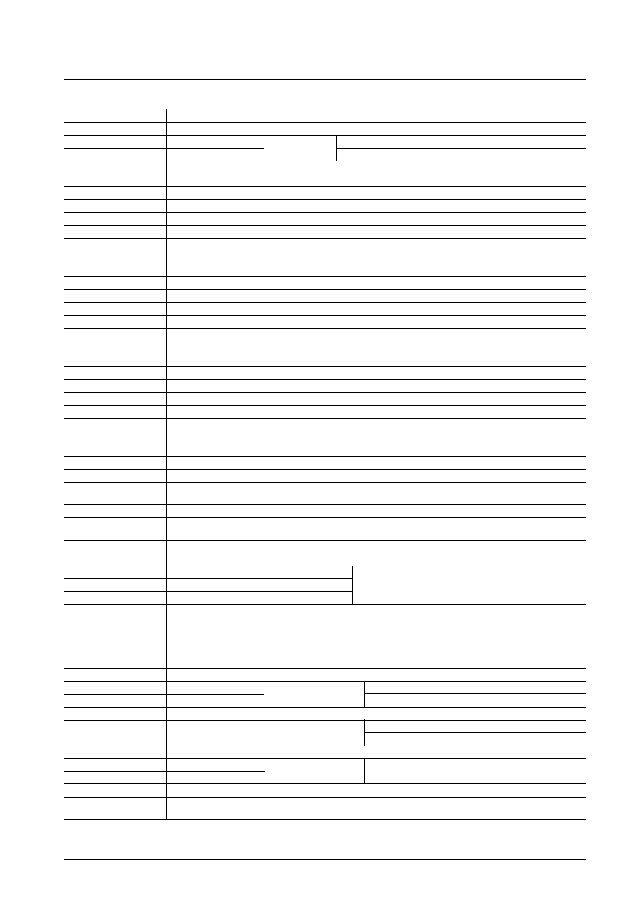
Pin Functions
Pin No.
Pin name
I/O
State during a reset
Function
1
AVDD1
—
Analog system power supply 1
2
SLCO
AO
—
Slice level control
Slice level control output
3
EFMIN
AI
—
RF signal input
4
RF
AO
—
RF signal output
5
LPF
AO
—
RF signal DC level detection low-pass filter capacitor connection
6
JITTC
AI
—
Jitter detection capacitor connection
7
AIN
AI
—
A signal input
8
CIN
AI
—
C signal input
9
BIN
AI
—
B signal input
10
DIN
AI
—
D signal input
11
FEC
AO
—
FE signal low-pass filter capacitor connection
12
PHLPF/RFMON
AO
ZHI
IC internal analog signal monitor
13
VREF
AO
AVDD1/2
VREF voltage output
14
EIN
AI
—
E signal input
15
FIN
AI
—
F signal input
16
TEC
AO
—
TE signal low-pass filter capacitor connection
17
TE
AO
—
TE signal output
18
TEIN
AI
—
TE signal input used for TES signal generation
19
LDD
AO
—
Laser power control signal output
20
LDS
AI
—
Laser power detection signal input
21
FDO
AO
AVDD2/2
Focus control signal output. D/A converter output
22
TDO
AO
AVDD2/2
Tracking control signal output. D/A converter output
23
SLDO
AO
AVDD2/2
Sled control signal output. D/A converter output
24
SPDO
AO
AVDD2/2
Spindle control signal output. D/A converter output
25
AVSS
—
Analog system ground. This pin must be connected to the 0 V level.
26
AVDD2
—
Analog system power supply 2
27
DVDD
—
Digital system power supply
28
DVSS
—
Digital system ground. This pin must be connected to the 0 V level.
29
VPB
O
H
Rough servo/phase control automatic switching monitor output
High: rough servo, low: phase servo
30
DEFECT
O
L
Defect signal output
31
FSEQ
O
L
Detected sync signal output. This signal is high when the sync signal detected from the EFM
signal and the internally generated sync signal agree.
32
EFLG
O
L
C1/C2 error correction monitor output
33
FSX
O
L
7.35 kHz synchronization output signal. This output is only provided in CLV mode.
34
CONT1
I/O
Input
General-purpose I/O 1
These pins are controlled by the microcontroller.
35
CONT2
I/O
Input
General-purpose I/O 2
If unused, these pins must either be set to input mode and
36
CONT3
I/O
Input
General-purpose I/O 3
connected to the 0 V level or set to output mode and left open.
External de-emphasis setting/internal signal monitor 1. This pin is controlled by themicrocontroller.
37
MONI1
I/O
Input
If unused, this pin must either be set to input mode and connected to the 0 V level or set to
output mode and left open.
38
MONI2
O
L
Internal signal monitor 2
39
DOUT
O
L
Digital output. The output from this pin conforms to the EIAJ format. (SPDIF)
40
TEST
I
L
Test input. This pin must be connected to the 0 V level.
41
LVDD
—
Left channel D/A converter
Left channel power supply
42
LCHO
AO
LVDD/2
Left channel output
43
LRVSS
—
Left and right channel ground. This pin must be connected to the 0 V level.
44
RCHO
AO
RVDD/2
Right channel D/A converter
Right channel output
45
RVDD
—
Right channel power supply
46
XVSS
—
Digital system ground. This pin must be connected to the 0 V level.
47
XOUT
O
Oscillating
Crystal oscillator
Connections for a 16.9344 MHz oscillator element.
48
XIN
I
Oscillating
49
XVDD
—
Digital system power supply
50
IOMODE
I
—
Switches the output mode of the CONT4 to CONT6, MONI3 to MONI5, DRF, and WRQB pins.
Low: normal output, high: n-channel open-drain output
Continued on next page.
相关PDF资料 |
PDF描述 |
|---|---|
| LC78681E | SPECIALTY CONSUMER CIRCUIT, PQFP64 |
| LC78681KE-L | SPECIALTY CONSUMER CIRCUIT, PQFP64 |
| LC78681KE | SPECIALTY CONSUMER CIRCUIT, PQFP64 |
| LC7868E | SPECIALTY CONSUMER CIRCUIT, PQFP64 |
| LC7869E | SPECIALTY CONSUMER CIRCUIT, PQFP64 |
相关代理商/技术参数 |
参数描述 |
|---|---|
| LC7864KE | 制造商:未知厂家 制造商全称:未知厂家 功能描述: |
| LC7865E | 制造商:SANYO 制造商全称:Sanyo Semicon Device 功能描述:Digital Signal Processor for Compact Disc Players |
| LC7867 | 制造商:SANYO 制造商全称:Sanyo Semicon Device 功能描述:Digital Signal Processor for Compact Disc Players |
| LC7867E | 制造商:SANYO 制造商全称:Sanyo Semicon Device 功能描述:Digital Signal Processor for Compact Disc Players |
| LC786800E | 制造商:SANYO 制造商全称:Sanyo Semicon Device 功能描述:Compressed Audio signal Processor IC with USB host controller |
发布紧急采购,3分钟左右您将得到回复。