- 您现在的位置:买卖IC网 > PDF目录30736 > LC82161B-E SPECIALTY CONSUMER CIRCUIT, PQFP208 PDF资料下载
参数资料
| 型号: | LC82161B-E |
| 元件分类: | 消费家电 |
| 英文描述: | SPECIALTY CONSUMER CIRCUIT, PQFP208 |
| 封装: | SQFP-208 |
| 文件页数: | 14/19页 |
| 文件大小: | 225K |
| 代理商: | LC82161B-E |
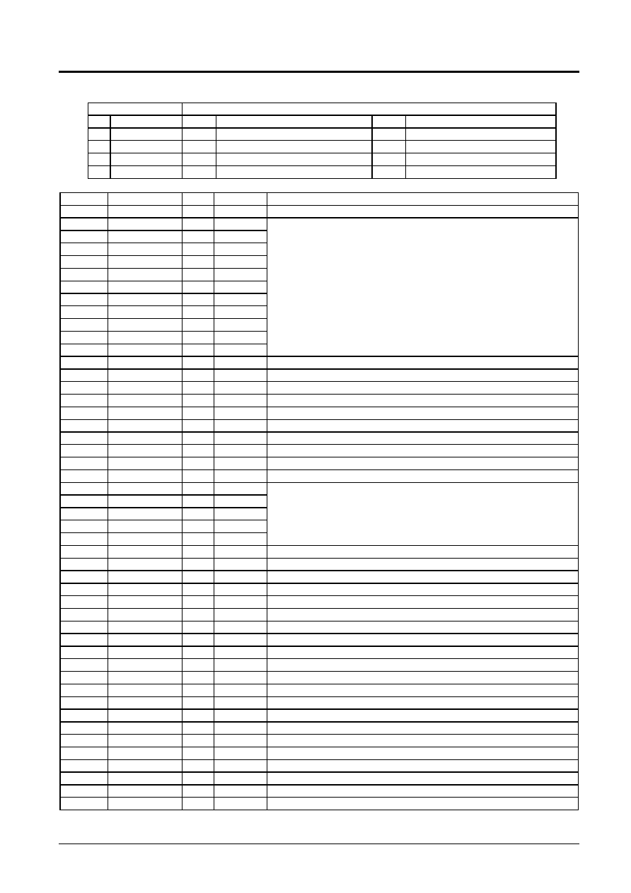
LC82161B-E
No.7775-4/19
Pin Functions
I/O
Pin type
I
Input pins
3IC
3.3 V CMOS inputs
3O8
3.3 V 8 mA output
O
Output pins
3IS
3.3 V Schmidt trigger inputs
3T4
3.3 V 4 mA tristate output
B
Bidirectional pins
3ICD
3.3 V CMOS inputs with pull-down resistor
3A
3.3 V analog
P
Power supply pins
3ICU
3.3 V CMOS inputs with pull-up resistor
2A
2.5 V analog
NC
Unused pins
3O4
3.3 V 4 mA outputs
X
Oscillator amplifier
Pin No.
Pin name
I/O
Pin type
Function
1
DGND
P
Digital system ground
2
A15
O
3O4
3
A14
O
3O4
4
A13
O
3O4
5
A12
O
3O4
6
A11
O
3O4
7
A10
O
3O4
8
A9
O
3O4
9
A8
O
3O4
10
A7
O
3O4
11
A6
O
3O4
12
A5
O
3O4
Address bus
13
TEST3
I
3ICD
Test
14
TEST2
I
3ICD
Test
15
TEST1
I
3ICD
Test
16
PVDD2
P
PLL power supply (+2.5 V)
17
PGND
P
PLL ground
18
RIN1
I
2A
PLL1 bias input
19
PLLI1
I
2A
PLL1 VCO input
20
PLLO1
O
2A
PLL1 charge pump output
21
TEST0
I
3ICD
Test
22
ROMBUSW
I
3ICD
Memory bus width selection
23
A4
O
3O4
24
A3
O
3O4
25
A2
O
3O4
26
A1
O
3O4
27
A0
O
3O4
Address bus
28
MWRLn
O
3O4
External memory write signal
29
MWRHn
O
3O4
External memory write signal
30
MRDn
O
3O4
External memory read signal
31
RESETn
I
3IS
Reset
32
XTAL1
I
X
Crystal oscillator connection (8.192 MHz)
33
XTAL2
O
X
34
DVDD3
P
Digital system power supply (+3.3 V)
35
DGND
P
Digital system ground
36
CS0n
O
3O4
External memory chip select 0
37
CS1n/PD4
B
3ICU/3T4
External memory chip select 1 or I/O port
38
CS2n/PD5
B
3ICU/3T4
External memory chip select 2 or I/O port
39
CS3n/PD6
B
3ICU/3T4
External memory chip select 3 or I/O port
40
DRCS1n
O
3O4
SDRAM chip select 1
41
DRCS0n
O
3O4
SDRAM chip select 0
42
RASn
O
3O4
Row address strobe
43
CASn
O
3O4
Column address strobe
44
DRCLK
O
3O8
SDRAM clock
45
DRWE
O
3O4
SDRAM write enable
46
DQM1
O
3O4
SDRAM byte mask 1
47
DQM0
O
3O4
SDRAM byte mask 0
48
M1_TXEN
O
3O4
MAC1 transmit enable
Continued on next page.
相关PDF资料 |
PDF描述 |
|---|---|
| LC8220 | SPECIALTY CONSUMER CIRCUIT, PQFP160 |
| LC82210 | SPECIALTY CONSUMER CIRCUIT, PQFP100 |
| LC82220 | SPECIALTY CONSUMER CIRCUIT, PQFP128 |
| LC8230 | SPECIALTY CONSUMER CIRCUIT, PQFP100 |
| LC823231 | SPECIALTY CONSUMER CIRCUIT, PQFP64 |
相关代理商/技术参数 |
参数描述 |
|---|---|
| LC821621-E | 制造商:ON Semiconductor 功能描述:VOIP PROCESSOR - Trays |
| LC82162BL-E | 制造商:ON Semiconductor 功能描述:VOIP PROCESSOR - Trays |
| LC82162B-R1000-E | 制造商:ON Semiconductor 功能描述:VOIP PROCESSOR - Trays 制造商:ON Semiconductor 功能描述:Processors - Application Specialized |
| LC8220 | 制造商:SANYO 制造商全称:Sanyo Semicon Device 功能描述:JPEG Still Color Image Compression/Decompression LSI |
| LC82-2001G | 制造商:SEI Stackpole Electronics Inc 功能描述: |
发布紧急采购,3分钟左右您将得到回复。