- 您现在的位置:买卖IC网 > PDF目录4567 > LFXP20E-5FN484C (Lattice Semiconductor Corporation)IC FPGA 19.7KLUTS 340I/O 484-BGA PDF资料下载
参数资料
| 型号: | LFXP20E-5FN484C |
| 厂商: | Lattice Semiconductor Corporation |
| 文件页数: | 144/397页 |
| 文件大小: | 0K |
| 描述: | IC FPGA 19.7KLUTS 340I/O 484-BGA |
| 标准包装: | 60 |
| 系列: | XP |
| 逻辑元件/单元数: | 20000 |
| RAM 位总计: | 405504 |
| 输入/输出数: | 340 |
| 电源电压: | 1.14 V ~ 1.26 V |
| 安装类型: | 表面贴装 |
| 工作温度: | 0°C ~ 85°C |
| 封装/外壳: | 484-BBGA |
| 供应商设备封装: | 484-FPBGA(23x23) |
第1页第2页第3页第4页第5页第6页第7页第8页第9页第10页第11页第12页第13页第14页第15页第16页第17页第18页第19页第20页第21页第22页第23页第24页第25页第26页第27页第28页第29页第30页第31页第32页第33页第34页第35页第36页第37页第38页第39页第40页第41页第42页第43页第44页第45页第46页第47页第48页第49页第50页第51页第52页第53页第54页第55页第56页第57页第58页第59页第60页第61页第62页第63页第64页第65页第66页第67页第68页第69页第70页第71页第72页第73页第74页第75页第76页第77页第78页第79页第80页第81页第82页第83页第84页第85页第86页第87页第88页第89页第90页第91页第92页第93页第94页第95页第96页第97页第98页第99页第100页第101页第102页第103页第104页第105页第106页第107页第108页第109页第110页第111页第112页第113页第114页第115页第116页第117页第118页第119页第120页第121页第122页第123页第124页第125页第126页第127页第128页第129页第130页第131页第132页第133页第134页第135页第136页第137页第138页第139页第140页第141页第142页第143页当前第144页第145页第146页第147页第148页第149页第150页第151页第152页第153页第154页第155页第156页第157页第158页第159页第160页第161页第162页第163页第164页第165页第166页第167页第168页第169页第170页第171页第172页第173页第174页第175页第176页第177页第178页第179页第180页第181页第182页第183页第184页第185页第186页第187页第188页第189页第190页第191页第192页第193页第194页第195页第196页第197页第198页第199页第200页第201页第202页第203页第204页第205页第206页第207页第208页第209页第210页第211页第212页第213页第214页第215页第216页第217页第218页第219页第220页第221页第222页第223页第224页第225页第226页第227页第228页第229页第230页第231页第232页第233页第234页第235页第236页第237页第238页第239页第240页第241页第242页第243页第244页第245页第246页第247页第248页第249页第250页第251页第252页第253页第254页第255页第256页第257页第258页第259页第260页第261页第262页第263页第264页第265页第266页第267页第268页第269页第270页第271页第272页第273页第274页第275页第276页第277页第278页第279页第280页第281页第282页第283页第284页第285页第286页第287页第288页第289页第290页第291页第292页第293页第294页第295页第296页第297页第298页第299页第300页第301页第302页第303页第304页第305页第306页第307页第308页第309页第310页第311页第312页第313页第314页第315页第316页第317页第318页第319页第320页第321页第322页第323页第324页第325页第326页第327页第328页第329页第330页第331页第332页第333页第334页第335页第336页第337页第338页第339页第340页第341页第342页第343页第344页第345页第346页第347页第348页第349页第350页第351页第352页第353页第354页第355页第356页第357页第358页第359页第360页第361页第362页第363页第364页第365页第366页第367页第368页第369页第370页第371页第372页第373页第374页第375页第376页第377页第378页第379页第380页第381页第382页第383页第384页第385页第386页第387页第388页第389页第390页第391页第392页第393页第394页第395页第396页第397页
LatticeECP/EC and LatticeXP
Lattice Semiconductor
DDR Usage Guide
10-9
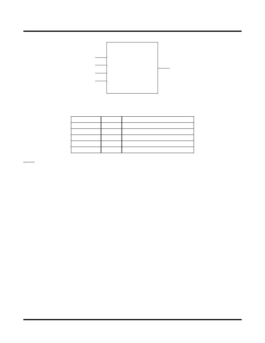
Figure 10-10. ODDRXB Symbol
Table 10-7 provides a description of all I/O ports associated with the ODDRXB primitive.
Table 10-7. ODDRXB Ports
Notes:
1. LSR should be held low during DDR Write operation. By default, the software will be implemented CE High
and LSR low.
2. DDR output and tristate registers do not have CE support. LSR is available for the tristate DDRX mode
(while reading). The LSR will default to set when used in the tristate mode.
3. CE and LSR support is available for the regular (non-DDR) output mode.
4. When asserting reset during DDR writes, it is important to keep in mind that this would only reset the FFs
and not the latches.
Memory Read Implementation
The LatticeECP/EC and LatticeXP devices contain a variety of features to simplify implementation of the read por-
tion of a DDR interface:
DLL compensated DQS delay elements
DDR input registers
Automatic DQS to system clock domain transfer circuitry
The LatticeECP/EC and LatticeXP device data sheets detail these circuit elements.
Three primitives in the Lattice ispLEVER
design tools represent the capability of these three elements. The DQS-
DLL represents the DLL used for calibration. The IDDRXB primitive represents the DDR input registers and clock
domain transfer registers. Finally, the DQSBUFB represents the DQS delay block and the clock polarity control
logic. These primitives are explained in more detail in the following sections of this document. Figure 10-11 illus-
trates how to hook these primitives together to implement the read portion of a DDR memory interface. The DDR
Software Primitives section describes each of the primitives and its instantiation in more detail. Appendices A and B
provide example code to implement the complete I/O section of a memory interface within a LatticeECP/EC or Lat-
ticeXP device.
Port Name
I/O
Definition
CLK
I
System CLK
DA
I
Data at the positive edge of the clock
DB
I
Data at the negative edge of the clock
LSR
I
Reset
Q
I
DDR data to the memory
Q
ODDRXB
CLK
DA
DB
LSR
相关PDF资料 |
PDF描述 |
|---|---|
| LFXP20C-5FN484C | IC FPGA 19.7KLUTS 340I/O 484-BGA |
| LFXP20C-5F484C | IC FPGA 19.7KLUTS 340I/O 484-BGA |
| LFEC33E-3FN672C | IC FPGA 32.8KLUTS 672FPBGA |
| LFECP33E-3FN484C | IC FPGA 32.8KLUTS 360I/O 484-BGA |
| RGM43DTMS | CONN EDGECARD 86POS R/A .156 SLD |
相关代理商/技术参数 |
参数描述 |
|---|---|
| LFXP217E5CF484C | 制造商:LATTICE 制造商全称:Lattice Semiconductor 功能描述:LatticeXP2 Family Data Sheet |
| LFXP217E5CF484I | 制造商:LATTICE 制造商全称:Lattice Semiconductor 功能描述:LatticeXP2 Family Data Sheet |
| LFXP217E5CF672C | 制造商:LATTICE 制造商全称:Lattice Semiconductor 功能描述:LatticeXP2 Family Data Sheet |
| LFXP217E5CF672I | 制造商:LATTICE 制造商全称:Lattice Semiconductor 功能描述:LatticeXP2 Family Data Sheet |
| LFXP217E5CFN484C | 制造商:LATTICE 制造商全称:Lattice Semiconductor 功能描述:LatticeXP2 Family Data Sheet |
发布紧急采购,3分钟左右您将得到回复。