- 您现在的位置:买卖IC网 > PDF目录67755 > LM12434CIWMX (NATIONAL SEMICONDUCTOR CORP) SPECIALTY ANALOG CIRCUIT, PDSO28 PDF资料下载
参数资料
| 型号: | LM12434CIWMX |
| 厂商: | NATIONAL SEMICONDUCTOR CORP |
| 元件分类: | 模拟信号调理 |
| 英文描述: | SPECIALTY ANALOG CIRCUIT, PDSO28 |
| 封装: | SOP-28 |
| 文件页数: | 71/80页 |
| 文件大小: | 1552K |
| 代理商: | LM12434CIWMX |
第1页第2页第3页第4页第5页第6页第7页第8页第9页第10页第11页第12页第13页第14页第15页第16页第17页第18页第19页第20页第21页第22页第23页第24页第25页第26页第27页第28页第29页第30页第31页第32页第33页第34页第35页第36页第37页第38页第39页第40页第41页第42页第43页第44页第45页第46页第47页第48页第49页第50页第51页第52页第53页第54页第55页第56页第57页第58页第59页第60页第61页第62页第63页第64页第65页第66页第67页第68页第69页第70页当前第71页第72页第73页第74页第75页第76页第77页第78页第79页第80页
80 Analog Considerations
81 REFERENCE VOLTAGE
The difference between the voltages applied to the VREFa
and VREFb is the analog input voltage span (the difference
between the voltages applied across two multiplexer inputs
or the voltage applied to one of the multiplexer inputs and
analog ground over which 4095 positive and 4096 negative
codes exist) The voltage sources driving VREFa or VREFb
must have very low output impedance and noise The circuit
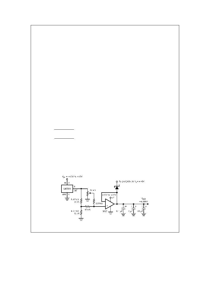
in
Figure 19 is an example of a very stable reference appro-
priate for use with the LM12434 and LM12 L 438
The ADC can be used in either ratiometric or absolute refer-
ence applications In ratiometric systems the analog input
voltage is proportional to the voltage used for the ADC’s
reference voltage When this voltage is the system power
supply the VREFa pin is connected to VAa and VREFb is
connected to GND This technique relaxes the system refer-
ence stability requirements because the analog input volt-
age and the ADC reference voltage move together This
maintains the same output code for given input conditions
For absolute accuracy where the analog input voltage var-
ies between very specific voltage limits a time and tempera-
ture stable voltage source can be connected to the refer-
ence inputs Typically the reference voltage’s magnitude
will require an initial adjustment to null reference voltage
induced full-scale errors
82 INPUT RANGE
The LM12434 and LM12 L 438’s fully differential ADC and
reference voltage inputs generate a two’s-complement out-
put that is found by using the equation below
output code e
VINa b VINb
VREFa b VREFb
(4096) b
(12-bit)
output code e
VINa b VINb
VREFa b VREFb
(256) b
(8-bit)
Round up to the next integer value between b4096 to 4095
for 12-bit resolution and between b256 to 255 for 8-bit res-
olution if the result of the above equation is not a whole
number As an example VREFa e 25V VREFb e 1V
VINa e 15V and VINb e GND The 12-bit a sign output
code is positive full-scale or 0111111111111 If VREFa
e
5V VREFb e 1V VINa e 3V and VINb e GND the
12-bit a sign output code is 0110000000000
83 INPUT CURRENT
A charging current flows into or out of (depending on the
input voltage polarity) the analog input pins IN0 – IN7 at the
start of the analog input acquisition time (tACQ) This cur-
rent’s peak value will depend on the actual input voltage
applied
84 INPUT SOURCE RESISTANCE
For low impedance voltage sources (k60X for 8 MHz oper-
ation) the input charging current will decay before the end
of the SH’s acquisition time to a value that will not intro-
duce any conversion errors For higher source impedances
the SH’s acquisition time can be increased As an exam-
ple operating with a 8 MHz clock frequency and maximum
acquisition time the LM12434 and LM12438’s analog inputs
can handle source impedances as high as 417 kX Refer to
Section 621 Instruction RAM ‘‘00’’ Bits 12 – 15 for further
information
85 INPUT BYPASS CAPACITANCE
External capacitors (001 mF – 01 mF) can be connected be-
tween the analog input pins IN0 – IN7 and analog ground to
filter any noise caused by inductive pickup associated with
long input leads These capacitors will not degrade the con-
version accuracy
86 INPUT NOISE
The leads to each of the analog multiplexer input pins
should be kept as short as possible This will minimize input
noise and clock frequency coupling that can cause conver-
sion errors Input filtering can be used to reduce the effects
of the noise sources
87 POWER SUPPLY CONSIDERATIONS
Decoupling and bypassing the power supply on a high reso-
lution ADC is an important design task Noise spikes on the
VAa (analog supply) or VDa (digital supply) can cause
conversion errors The analog comparator used in the ADC
will respond to power supply noise and will make erroneous
conversion decisions The DAS is especially sensitive to
power supply spikes that occur during the auto-zero or lin-
earity calibration cycles
Tantalum
Ceramic
TLH11879 – 20
FIGURE 19 Low Drift Extremely Stable Reference Circuit
73
相关PDF资料 |
PDF描述 |
|---|---|
| LM12L438CIWMX | SPECIALTY ANALOG CIRCUIT, PDSO28 |
| LM20323AMHX | 6 A SWITCHING REGULATOR, 570 kHz SWITCHING FREQ-MAX, PDSO20 |
| LM20323AMHE | 6 A SWITCHING REGULATOR, 570 kHz SWITCHING FREQ-MAX, PDSO20 |
| LM20323AMH | 6 A SWITCHING REGULATOR, 570 kHz SWITCHING FREQ-MAX, PDSO20 |
| LM22677QTJ-5.0 | 8.75 A SWITCHING REGULATOR, 600 kHz SWITCHING FREQ-MAX, PSSO7 |
相关代理商/技术参数 |
参数描述 |
|---|---|
| LM12438CIV | 制造商:NSC 制造商全称:National Semiconductor 功能描述:Sign Data Acquisition System with Serial I/O and Self-Calibration |
| LM12438CIWM | 制造商:NSC 制造商全称:National Semiconductor 功能描述:Sign Data Acquisition System with Serial I/O and Self-Calibration |
| LM12454 | 制造商:未知厂家 制造商全称:未知厂家 功能描述:General Purpose Controller Z84C15 |
| LM12454_06 | 制造商:NSC 制造商全称:National Semiconductor 功能描述:12-Bit + Sign Data Acquisition System with Self-Calibration |
| LM12454A WAF | 制造商:Texas Instruments 功能描述: |
发布紧急采购,3分钟左右您将得到回复。