- 您现在的位置:买卖IC网 > PDF目录44529 > LM12458CIVF/NOPB (NATIONAL SEMICONDUCTOR CORP) SPECIALTY ANALOG CIRCUIT, PQFP44 PDF资料下载
参数资料
| 型号: | LM12458CIVF/NOPB |
| 厂商: | NATIONAL SEMICONDUCTOR CORP |
| 元件分类: | 模拟信号调理 |
| 英文描述: | SPECIALTY ANALOG CIRCUIT, PQFP44 |
| 封装: | PLASTIC, QFP-44 |
| 文件页数: | 21/36页 |
| 文件大小: | 1195K |
| 代理商: | LM12458CIVF/NOPB |
第1页第2页第3页第4页第5页第6页第7页第8页第9页第10页第11页第12页第13页第14页第15页第16页第17页第18页第19页第20页当前第21页第22页第23页第24页第25页第26页第27页第28页第29页第30页第31页第32页第33页第34页第35页第36页
2.0 Internal User-Programmable
Registers (Continued)
mand (“1”) disconnects the external clock from the internal
circuitry, decreases the LM12(H)454/8’s internal analog cir-
cuitry power supply current, and preserves all internal RAM
contents. After writing a “0” to the Standby bit, the
LM12(H)454/8 returns to an operating state identical to that
caused by exercising the RESET bit. A Standby completion
interrupt is issued after a power-up completion delay that
allows the analog circuitry to settle. The Sequencer should
be restarted only after the Standby completion is issued. The
Instruction RAM can still be accessed through read and write
operations while the LM12(H)454/8 are in Standby Mode.
Bit 5 is the Channel Address Mask. If Bit 5 is set to a “1”, Bits
13–15 in the conversion FIFO will be equal to the sign bit (Bit
12) of the conversion data. Resetting Bit 5 to a “0” causes
conversion data Bits 13 through 15 to hold the instruction
pointer value of the instruction to which the conversion data
belongs.
Bit 6 is used to select a “short” auto-zero correction for every
conversion. The Sequencer automatically inserts an auto-
zero before every conversion or “watchdog” comparison if
Bit 6 is set to “1”. No automatic correction will be performed
if Bit 6 is reset to “0”.
The LM12(H)454/8’s offset voltage, after calibration, has a
typical drift of 0.1 LSB over a temperature range of 40C to
+85C. This small drift is less than the variability of the
change in offset that can occur when using the auto-zero
correction with each conversion. This variability is the result
of using only one sample of the offset voltage to create a
correction value. This variability decreases when using the
full calibration mode because eight samples of the offset
voltage are taken, averaged, and used to create a correction
value.
Bit 7 is used to program the SYNC pin (29) to operate as
either an input or an output. The SYNC pin becomes an
output when Bit 7 is a “1” and an input when Bit 7 is a “0”.
With SYNC programmed as an input, the rising edge of any
logic signal applied to pin 29 will start a conversion or
“watchdog” comparison. Programmed as an output, the logic
level at pin 29 will go high at the start of a conversion or
“watchdog” comparison and remain high until either have
finished. See Instruction RAM “00”, Bit 8.
Bits 8 and 9 form the RAM Pointer that is used to select
each of a 48-bit instruction’s three 16-bit sections during
read or write actions. A “00” selects Instruction RAM section
one, “01” selects section two, and “10” selects section three.
Bit 10 activates the Test mode that is used only during
production testing. Leave this bit reset to “0”.
Bit 11 is the Diagnostic bit and is available only in the
LM12(H)458. It can be activated by setting it to a “1” (the Test
bit must be reset to a “0”). The Diagnostic mode, along with
a correctly chosen instruction, allows verification that the
LM12(H)458’s ADC is performing correctly. When activated,
the inverting and non-inverting inputs are connected as
shown in Table 1. As an example, an instruction with “001”
for both V
IN+ and VIN while using the Diagnostic mode
typically results in a full-scale output.
2.3 INTERRUPTS
The LM12454 and LM12(H)458 have eight possible inter-
rupts, all with the same priority. Any of these interrupts will
cause a hardware interrupt to appear on the INT pin (31) if
they are not masked (by the Interrupt Enable register). The
Interrupt Status register is then read to determine which of
the eight interrupts has been issued.
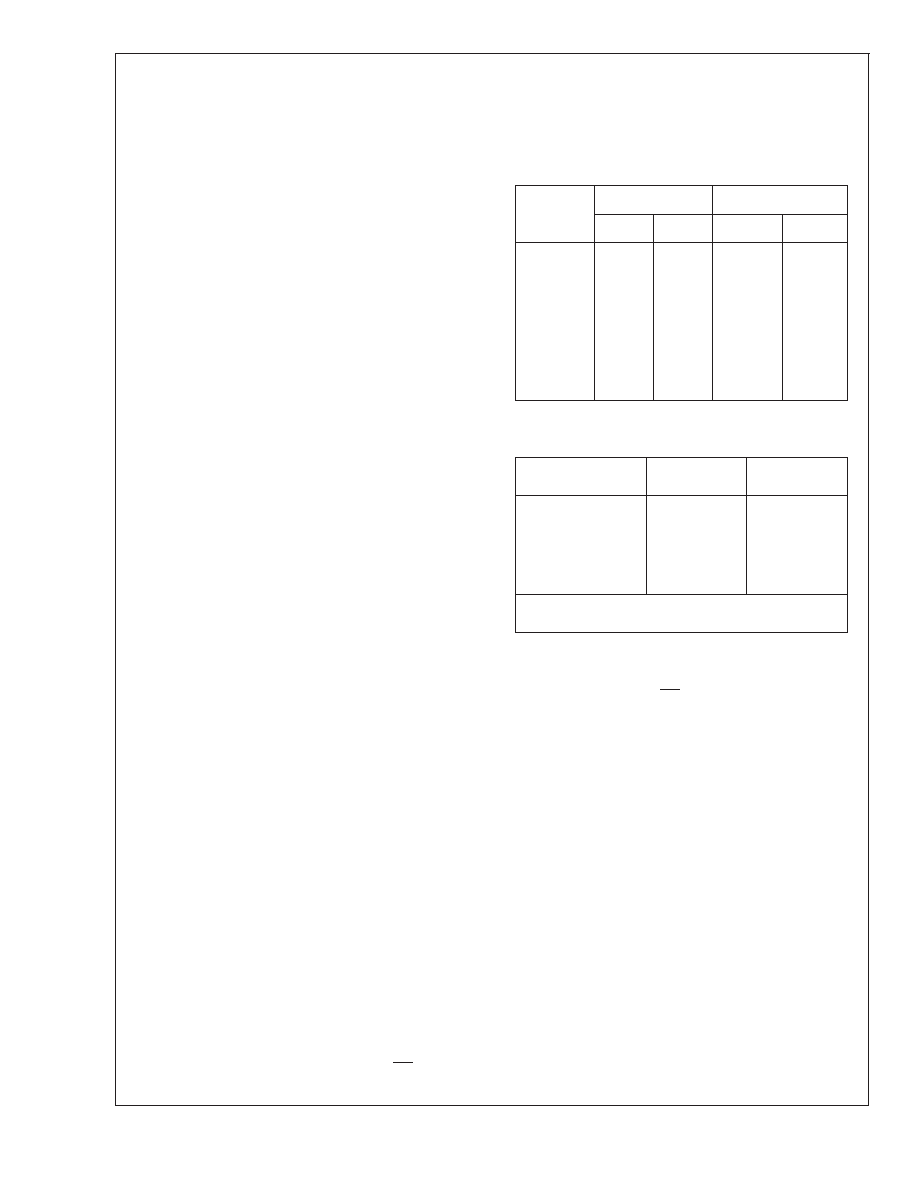
TABLE 1. LM12(H)458 Input Multiplexer
Channel Configuration Showing Normal
Mode and Diagnostic Mode
Channel
Selection
Data
Normal Mode
Diagnostic Mode
V
IN+
V
IN
V
IN+
V
IN
000
IN0
GND
V
REFOUT
GND
001
IN1
V
REF+
V
REF
010
IN2
011
IN3
100
IN4
101
IN5
110
IN6
111
IN7
TABLE 2. LM12454 Input Multiplexer
Channel Configuration
Channel Selection
Data
MUX+
MUX
000
IN0
GND
001
IN1
010
IN2
011
IN3
1XX
OPEN
NOTE: The LM12(H)454 is no longer available.
Information shown for reference only.
The Interrupt Status register, 1010 (A4–A1, BW = 0) or
1010x (A4–A0, BW = 1) must be cleared by reading it after
writing to the Interrupt Enable register. This removes any
spurious interrupts on the INT pin generated during an Inter-
rupt Enable register access.
Interrupt 0 is generated whenever the analog input voltage
on a selected multiplexer channel crosses a limit while the
LM12(H)454/8 are operating in the “watchdog” comparison
mode. Two sequential comparisons are made when the
LM12(H)454/8 are executing a “watchdog” instruction. De-
pending on the logic state of Bit 9 in the Instruction RAM’s
second and third sections, an interrupt will be generated
either when the input signal’s magnitude is greater than or
less than the programmable limits. (See the Instruction
RAM, Bit 9 description.) The Limit Status register will indicate
which preprogrammed limit, #1 or #2 and which instruction
was executing when the limit was crossed.
Interrupt 1 is generated when the Sequencer reaches the
instruction counter value specified in the Interrupt Enable
register’s bits 8–10. This flag appears before the instruc-
tion’s execution.
Interrupt 2 is activated when the Conversion FIFO holds a
number of conversions equal to the programmable value
stored in the Interrupt Enable register’s Bits 11–15. This
value ranges from 0001 to 1111, representing 1 to 31 con-
versions stored in the FIFO. A user-programmed value of
0000 has no meaning. See Section 3.0 for more FIFO infor-
mation.
LM12454/LM12458/LM12H458
www.national.com
28
相关PDF资料 |
PDF描述 |
|---|---|
| LM129AGMW8 | 1-OUTPUT TWO TERM VOLTAGE REFERENCE, 6.9 V, UUC |
| LM12H458MW/883 | SPECIALTY ANALOG CIRCUIT, CQFP44 |
| 5962-9319502MXC | SPECIALTY ANALOG CIRCUIT, CQCC44 |
| LM12L454CIV | SPECIALTY ANALOG CIRCUIT, PQCC44 |
| LM134MWC | SPECIALTY ANALOG CIRCUIT, UUC |
相关代理商/技术参数 |
参数描述 |
|---|---|
| LM12458CIVX | 功能描述:模数转换器 - ADC RoHS:否 制造商:Texas Instruments 通道数量:2 结构:Sigma-Delta 转换速率:125 SPs to 8 KSPs 分辨率:24 bit 输入类型:Differential 信噪比:107 dB 接口类型:SPI 工作电源电压:1.7 V to 3.6 V, 2.7 V to 5.25 V 最大工作温度:+ 85 C 安装风格:SMD/SMT 封装 / 箱体:VQFN-32 |
| LM12458CIVX/NOPB | 功能描述:模数转换器 - ADC RoHS:否 制造商:Texas Instruments 通道数量:2 结构:Sigma-Delta 转换速率:125 SPs to 8 KSPs 分辨率:24 bit 输入类型:Differential 信噪比:107 dB 接口类型:SPI 工作电源电压:1.7 V to 3.6 V, 2.7 V to 5.25 V 最大工作温度:+ 85 C 安装风格:SMD/SMT 封装 / 箱体:VQFN-32 |
| LM12458CMEL/883 | 制造商:未知厂家 制造商全称:未知厂家 功能描述:Single-Ended Data Acquisition System |
| LM12458MEL/883 | 制造商:未知厂家 制造商全称:未知厂家 功能描述:Single-Ended Data Acquisition System |
| LM12458MW/883 | 制造商:未知厂家 制造商全称:未知厂家 功能描述:Single-Ended Data Acquisition System |
发布紧急采购,3分钟左右您将得到回复。