- 您现在的位置:买卖IC网 > PDF目录44529 > LM12458CIVF/NOPB (NATIONAL SEMICONDUCTOR CORP) SPECIALTY ANALOG CIRCUIT, PQFP44 PDF资料下载
参数资料
| 型号: | LM12458CIVF/NOPB |
| 厂商: | NATIONAL SEMICONDUCTOR CORP |
| 元件分类: | 模拟信号调理 |
| 英文描述: | SPECIALTY ANALOG CIRCUIT, PQFP44 |
| 封装: | PLASTIC, QFP-44 |
| 文件页数: | 27/36页 |
| 文件大小: | 1195K |
| 代理商: | LM12458CIVF/NOPB |
第1页第2页第3页第4页第5页第6页第7页第8页第9页第10页第11页第12页第13页第14页第15页第16页第17页第18页第19页第20页第21页第22页第23页第24页第25页第26页当前第27页第28页第29页第30页第31页第32页第33页第34页第35页第36页
6.0 Design Considerations
6.1 REFERENCE VOLTAGE
The difference in the voltages applied to the V
REF+ and
V
REF defines the analog input voltage span (the difference
between the voltages applied between two multiplexer inputs
or the voltage applied to one of the multiplexer inputs and
analog ground), over which 4095 positive and 4096 negative
codes exist. The voltage sources driving V
REF+ or VREF
must have very low output impedance and noise.
The ADC can be used in either ratiometric or absolute refer-
ence applications. In ratiometric systems, the analog input
voltage is proportional to the voltage used for the ADC’s
reference voltage. When this voltage is the system power
supply, the V
REF+ pin is connected to VA+ and VREF is
connected to GND. This technique relaxes the system refer-
ence stability requirements because the analog input voltage
and the ADC reference voltage move together. This main-
tains the same output code for given input conditions.
For absolute accuracy, where the analog input voltage varies
between very specific voltage limits, a time and temperature
stable voltage source can be connected to the reference
inputs. Typically, the reference voltage’s magnitude will re-
quire an initial adjustment to null reference voltage induced
full-scale errors.
When using the LM12(H)454/8’s internal 2.5V bandgap ref-
erence, a parallel combination of a 100 F capacitor and a
0.1 F capacitor connected to the V
REFOUT pin is recom-
mended for low noise operation. When left unconnected, the
reference remains stable without a bypass capacitor. How-
ever, ensure that stray capacitance at the V
REFOUT pin re-
mains below 50 pF.
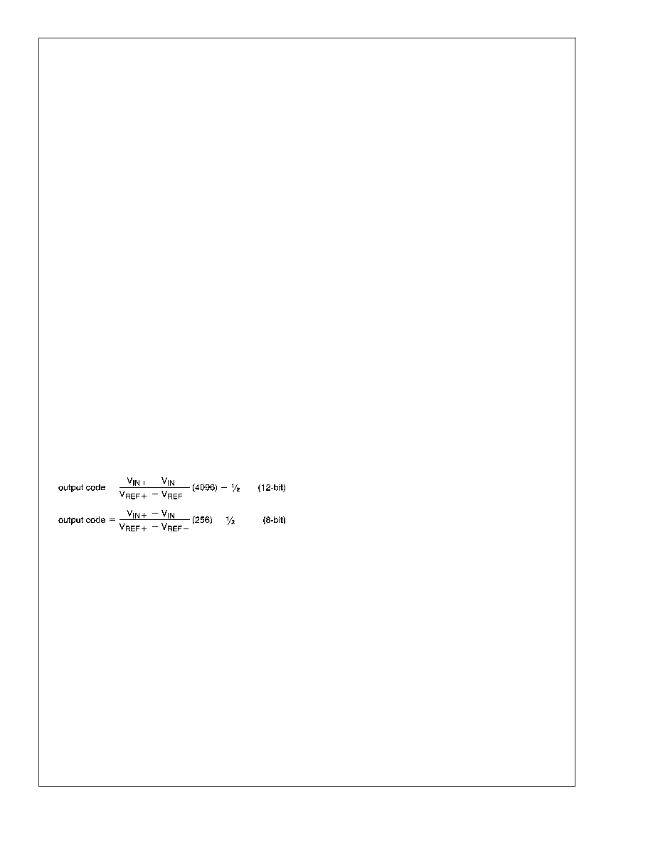
6.2 INPUT RANGE
The LM12(H)454/8’s fully differential ADC and reference
voltage inputs generate a two’s-complement output that is
found by using the equation below.
Round up to the next integer value between 4096 to 4095
for 12-bit resolution and between 256 to 255 for 8-bit reso-
lution if the result of the above equation is not a whole
number. As an example, V
REF+ = 2.5V, VREF =1V, VIN+ =
1.5V and V
IN = GND. The 12-bit + sign output code is
positive full-scale, or 0,1111,1111,1111. If V
REF+ =5V, VREF
=1V, V
IN+ = 3V, and VIN = GND, the 12-bit + sign output
code is 0,1100,0000,0000.
6.3 INPUT CURRENT
A charging current flows into or out of (depending on the
input voltage polarity) the analog input pins, IN0–IN7 at the
start of the analog input acquisition time (t
ACQ). This cur-
rent’s peak value will depend on the actual input voltage
applied. This charging current causes voltage spikes at the
inputs. This voltage spikes will not corrupt the conversion
results.
6.4 INPUT SOURCE RESISTANCE
For low impedance voltage sources (<100
for 5 MHz
operation and <60
for 8 MHz operation), the input charging
current will decay, before the end of the S/H’s acquisition
time, to a value that will not introduce any conversion errors.
For higher source impedances, the S/H’s acquisition time
can be increased. As an example, operating witha5MHz
clock
frequency
and
maximum
acquisition
time,
the
LM12(H)454/8’s analog inputs can handle source imped-
ance as high as 6.67 k
. When operating at 8 MHz and
maximum acquisition time, the LM12H454/8’s analog inputs
can handle source impedance as high as 4.17 k
. Refer to
Section 2.1, Instruction RAM “00”, Bits 12–15 for further
information.
6.5 INPUT BYPASS CAPACITANCE
External capacitors (0.01 F to 0.1 F) can be connected
between the analog input pins, IN0–IN7, and analog ground
to filter any noise caused by inductive pickup associated with
long input leads. It will not degrade the conversion accuracy.
6.6 NOISE
The leads to each of the analog multiplexer input pins should
be kept as short as possible. This will minimize input noise
and clock frequency coupling that can cause conversion
errors. Input filtering can be used to reduce the effects of the
noise sources.
6.7 POWER SUPPLIES
Noise spikes on the V
A+ and VD+ supply lines can cause
conversion errors; the comparator will respond to the noise.
The ADC is especially sensitive to any power supply spikes
that occur during the auto-zero or linearity correction. Low
inductance tantalum capacitors of 10 F or greater paral-
leled with 0.1 F monolithic ceramic capacitors are recom-
mended for supply bypassing. Separate bypass capacitors
should be used for the V
A+ and VD+ supplies and placed as
close as possible to these pins.
6.8 GROUNDING
The LM12(H)454/8’s nominal performance can be maxi-
mized through proper grounding techniques. These include
the use of a single ground plane and meticulously separating
analog and digital areas of the board. The use of separate
analog and digital digital planes within the same board area
generally provides best performance. All components that
handle digital signals should be placed within the digital area
of the board, as defined by the digital power plane, while all
analog components should be placed in the analog area of
the board. Such placement and the routing of analog and
digital signal lines within their own respective board areas
greatly reduces the occurrence of ground loops and noise.
This will also minimize EMI/RFI radiation and susceptibility.
It is recommended that stray capacitance between the ana-
log inputs or outputs, including the reference pins, be kept to
a minimum by increasing the clearance (+1/16th inch) be-
tween the analog signal and reference pins and the ground
plane.
6.9 CLOCK SIGNAL CONSIDERATIONS
The LM12(H)458’s performance is optimized by routing the
analog input/output and reference signal conductors (pins
34–44) as far as possible from the conductor that carries the
clock signal to pin 23.
Avoid overshoot and undershoot on the clock line by treating
this line as a transmission line (use proper termination tech-
LM12454/LM12458/LM12H458
www.national.com
33
相关PDF资料 |
PDF描述 |
|---|---|
| LM129AGMW8 | 1-OUTPUT TWO TERM VOLTAGE REFERENCE, 6.9 V, UUC |
| LM12H458MW/883 | SPECIALTY ANALOG CIRCUIT, CQFP44 |
| 5962-9319502MXC | SPECIALTY ANALOG CIRCUIT, CQCC44 |
| LM12L454CIV | SPECIALTY ANALOG CIRCUIT, PQCC44 |
| LM134MWC | SPECIALTY ANALOG CIRCUIT, UUC |
相关代理商/技术参数 |
参数描述 |
|---|---|
| LM12458CIVX | 功能描述:模数转换器 - ADC RoHS:否 制造商:Texas Instruments 通道数量:2 结构:Sigma-Delta 转换速率:125 SPs to 8 KSPs 分辨率:24 bit 输入类型:Differential 信噪比:107 dB 接口类型:SPI 工作电源电压:1.7 V to 3.6 V, 2.7 V to 5.25 V 最大工作温度:+ 85 C 安装风格:SMD/SMT 封装 / 箱体:VQFN-32 |
| LM12458CIVX/NOPB | 功能描述:模数转换器 - ADC RoHS:否 制造商:Texas Instruments 通道数量:2 结构:Sigma-Delta 转换速率:125 SPs to 8 KSPs 分辨率:24 bit 输入类型:Differential 信噪比:107 dB 接口类型:SPI 工作电源电压:1.7 V to 3.6 V, 2.7 V to 5.25 V 最大工作温度:+ 85 C 安装风格:SMD/SMT 封装 / 箱体:VQFN-32 |
| LM12458CMEL/883 | 制造商:未知厂家 制造商全称:未知厂家 功能描述:Single-Ended Data Acquisition System |
| LM12458MEL/883 | 制造商:未知厂家 制造商全称:未知厂家 功能描述:Single-Ended Data Acquisition System |
| LM12458MW/883 | 制造商:未知厂家 制造商全称:未知厂家 功能描述:Single-Ended Data Acquisition System |
发布紧急采购,3分钟左右您将得到回复。