- 您现在的位置:买卖IC网 > PDF目录30743 > LM1269NA/NOPB (NATIONAL SEMICONDUCTOR CORP) 3 CHANNEL, VIDEO PREAMPLIFIER, PDIP24 PDF资料下载
参数资料
| 型号: | LM1269NA/NOPB |
| 厂商: | NATIONAL SEMICONDUCTOR CORP |
| 元件分类: | 音频/视频放大 |
| 英文描述: | 3 CHANNEL, VIDEO PREAMPLIFIER, PDIP24 |
| 封装: | PLASTIC, DIP-24 |
| 文件页数: | 8/20页 |
| 文件大小: | 1676K |
| 代理商: | LM1269NA/NOPB |
PCB Layout
Micro-Controller Interface
The micro-controller interfaces to the LM1269 pre-amp via
an I
2C interface. The protocol of the interface begins with the
Start Pulse followed by a byte comprised of a seven-bit
Slave Device Address and a Read/Write bit as the LSB.
Therefore the address of the LM1269 for writing is DCh
(1101 1100) and the address for reading is DDh (1101 1101).
Figures 11, 12 show a write and read sequence across the
I
2C interface.
Write Sequence
The write sequence begins with a start condition which
consists of the master pulling SDA low while SCL is held
high. The slave device address is next sent. The address
byte is made up of an address of seven bits (7–1) and the
read/write bit (0). Bit 0 is low to indicate a write operation.
Each byte that is sent is followed by an acknowledge. When
SCL is high the master will release the SDA line. The slave
must pull SDA low to acknowledge. The address of the
register to be written to is sent next. Following the register
address and the acknowledge bit the data for the register is
sent. If bit 0 of register 0Ah is set low (default value) then the
LM1269 is set for the increment mode. In this mode when
more than one data byte is sent it is automatically incre-
mented into the next address location. See
Figure 11. Note
that each data byte is followed by an acknowledge bit.
Read Sequence
Read sequences are comprised of two I
2C transfer se-
quences. The first is a write sequence that only transfers the
address to be accessed. The second is a read sequence that
starts at the address transferred in the previous address
write access and incrementing to the next address upon
every data byte read. This is shown in
Figure 12.
The write sequence consists of the Start Pulse, the Slave
Device Address including the Read/Write bit (a zero, indicat-
ing a write), then its Acknowledge bit. The next byte is the
address to be accessed, followed by its Acknowledge bit and
the stop bit indicating the end of the address only write
access.
Next the read data access is performed beginning with the
Start Pulse, the Slave Device Address including the Read/
Write bit (a one, indicating a read) and the Acknowledge bit.
The next 8 bits will be the data read from the address
indicated by the write sequence. Subsequent read data
bytes will correspond to the next increment address loca-
tions. Each data byte is separated from the other data bytes
by an Acknowledge bit.
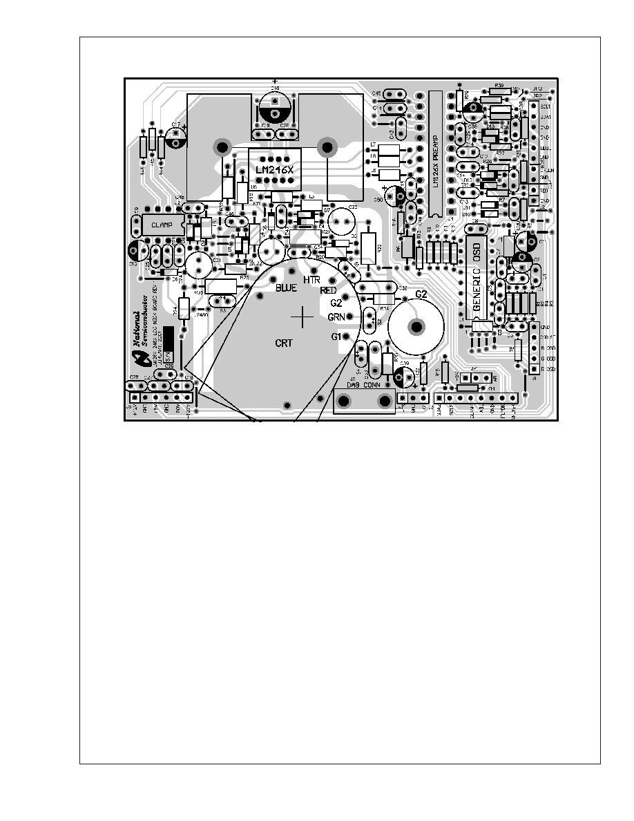
DS200099-31
FIGURE 10. LM126X/LM246X System Neck Board
LM1269
www.national.com
16
相关PDF资料 |
PDF描述 |
|---|---|
| LM1276AAA/NA | 1 CHANNEL, VIDEO PREAMPLIFIER, PDIP28 |
| LM1279AN/NOPB | 3 CHANNEL, VIDEO AMPLIFIER, PDIP20 |
| LM1279N/NOPB | 1 CHANNEL, VIDEO AMPLIFIER, PDIP20 |
| LM136A-2.5MD8 | 1-OUTPUT TWO TERM VOLTAGE REFERENCE, 5 V, UUC |
| LM136A-5.0MW8 | 1-OUTPUT TWO TERM VOLTAGE REFERENCE, 5 V, UUC |
相关代理商/技术参数 |
参数描述 |
|---|---|
| LM126H | 制造商:NSC 制造商全称:National Semiconductor 功能描述:VOLTAGE REGULATORS |
| LM126H/883B | 制造商:Texas Instruments 功能描述:IC,VOLT REGULATOR,FIXED,+-12V,BIPOLAR,CAN,10PIN,METAL |
| LM126H/883C | 制造商:Texas Instruments 功能描述: |
| LM1270 | 制造商:NSC 制造商全称:National Semiconductor 功能描述:Hi-Brite 200 MHz I2C Compatible RGB Image Enhancer with Video Auto Sizing |
| LM1270N | 制造商:NSC 制造商全称:National Semiconductor 功能描述:Hi-Brite 200 MHz I2C Compatible RGB Image Enhancer with Video Auto Sizing |
发布紧急采购,3分钟左右您将得到回复。