- 您现在的位置:买卖IC网 > PDF目录67755 > LM12L438CIWMX (NATIONAL SEMICONDUCTOR CORP) SPECIALTY ANALOG CIRCUIT, PDSO28 PDF资料下载
参数资料
| 型号: | LM12L438CIWMX |
| 厂商: | NATIONAL SEMICONDUCTOR CORP |
| 元件分类: | 模拟信号调理 |
| 英文描述: | SPECIALTY ANALOG CIRCUIT, PDSO28 |
| 封装: | SOP-28 |
| 文件页数: | 6/80页 |
| 文件大小: | 1552K |
| 代理商: | LM12L438CIWMX |
第1页第2页第3页第4页第5页当前第6页第7页第8页第9页第10页第11页第12页第13页第14页第15页第16页第17页第18页第19页第20页第21页第22页第23页第24页第25页第26页第27页第28页第29页第30页第31页第32页第33页第34页第35页第36页第37页第38页第39页第40页第41页第42页第43页第44页第45页第46页第47页第48页第49页第50页第51页第52页第53页第54页第55页第56页第57页第58页第59页第60页第61页第62页第63页第64页第65页第66页第67页第68页第69页第70页第71页第72页第73页第74页第75页第76页第77页第78页第79页第80页
20 Electrical Specifications (Continued)
24 NOTES ON SPECIFICATIONS
Note 1
Absolute Maximum Ratings indicate limits beyond which damage to the device may occur Operating Ratings indicate conditions for which the device is
functional but do not guarantee specific performance limits For guaranteed specifications and test conditions see the Electrical Characteristics The guaranteed
specifications apply only for the test conditions listed Some performance characteristics may degrade when the device is not operated under the listed test
conditions
Note 2
All voltages are measured with respect to GND unless otherwise specified GND specifies either AGND andor DGND and Va specifies either VAa and
or VDa
Note 3
When the input voltage (VIN) at any pin exceeds the power supply rails (VIN k GND or VIN l (VAa or VDa)) the current at that pin should be limited to
5 mA The 20 mA maximum package input current rating allows the voltage at any four pins with an input current of 5 mA to simultaneously exceed the power
supply voltages
Note 4
The maximum power dissipation must be derated at elevated temperatures and is dictated by TJmax (maximum junction temperature) HJA (package
junction to ambient thermal resistance) and TA (ambient temperature) The maximum allowable power dissipation at any temperature is PDmax e (TJmax b TA)
HJA or the number given in the Absolute Maximum Ratings whichever is lower For this device TJmax e 150 C and the typical thermal resistance (HJA) of the V
package when board mounted is 70 CW and in the WM package when board mounted is 60 CW
Note 5
Human body model 100 pF discharged through a 15 kX resistor
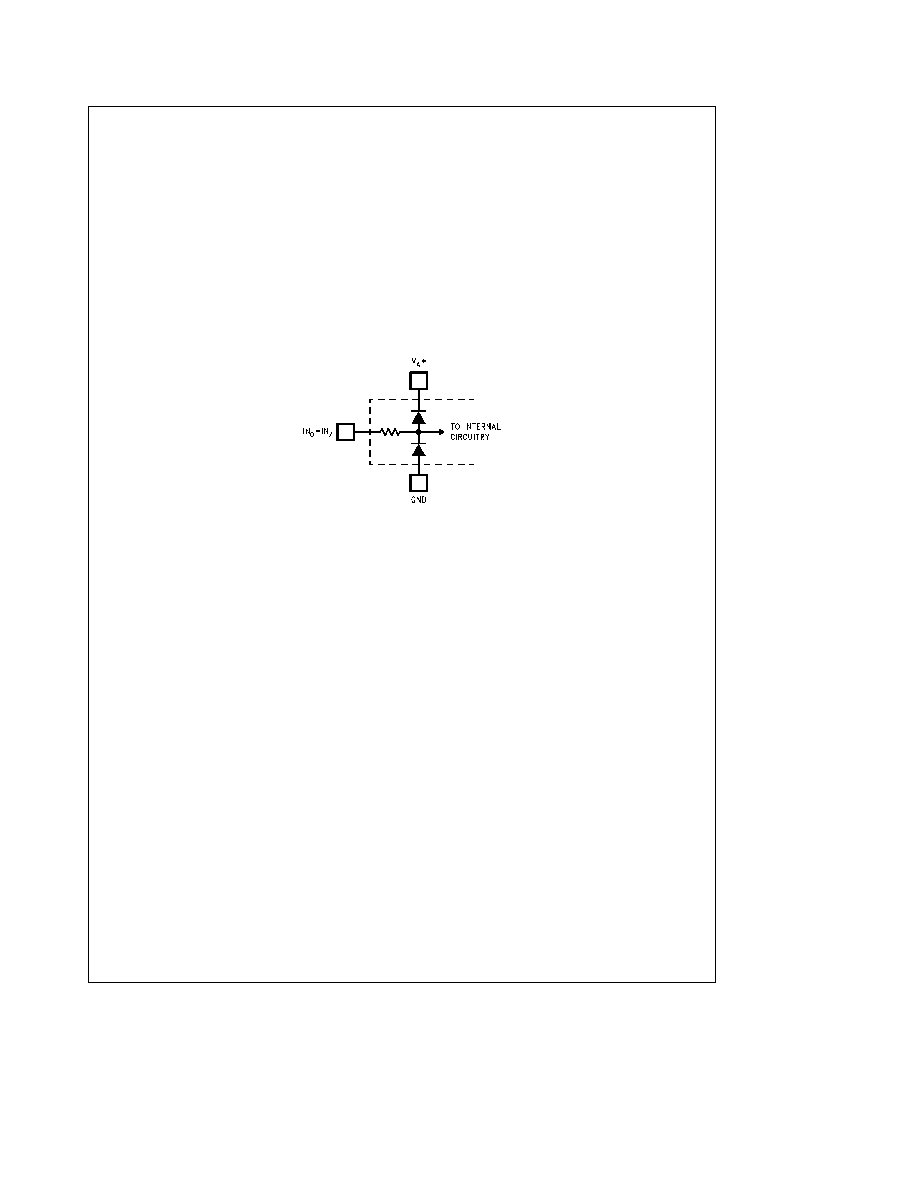
Note 6
Two on-chip diodes are tied to each analog input through a series resistor as shown below Input voltage magnitude up to 5V above VAa or 5V below
GND will not damage the part However errors in the AD conversion can occur if these diodes are forward biased by more than 100 mV As an example if VAa is
45 VDC the full-scale input voltage must be s46 VDC to ensure accurate conversions
TLH11879 – 5
Note 7
VAa and VDa must be connected together to the same power supply voltage and bypassed with separate capacitors at each Va pin to assure
conversioncomparison accuracy Refer to Section 80 for a detailed discussion on grounding the DAS
Note 8
Accuracy is guaranteed when operating the LM12434LM12 L 438 at fCLK e 8 MHz 6 MHz
Note 9
With the test condition for VREF (VREFa b VREFb) given as a4096V the 12-bit LSB is 1 mV and the 8-bit‘‘Watchdog’’ LSB is 19 mV
Note 10
Typicals are at TA e 25 C and represent most likely parametric norm
Note 11
Limits are guaranteed to National’s AOQL (Average Output Quality Level)
Note 12
Positive integral linearity error is defined as the deviation of the analog value expressed in LSBs from the straight line that passes through positive full-
scale and zero For negative integral linearity error the straight line passes through negative full-scale and zero (See
Figures 5b and 5c )
Note 13
Zero error is a measure of the deviation from the mid-scale voltage (a code of zero) expressed in LSB It is the average value of the code transitions
between b1to0and0to a1 (see
Figure 6 )
Note 14
The DC common-mode error is measured with both the inverted and non-inverted inputs shorted together and driven from 0V to 5V
33V
The
measured value is referred to the resulting output value when the inputs are driven with a 25V 165V signal
Note 15
Power Supply Sensitivity is measured after Auto-Zero andor Auto-Calibration cycle has been completed with VAa and VDa at the specified extremes
Note 16
VREFCM (Reference Voltage Common Mode Range) is defined as (VREFa a VREFb)2 See Figures 3 and 4
Note 17
The device self-calibration technique ensures linearity and offset errors as specified but noise inherent in the self-calibration process will result in a
repeatability uncertainty of g010 LSB
Note 18
The Throughput Rate is for a single instruction repeated continuously while reading data during conversions with a serial clock frequency fSCLK e 10 MHz
8 MHz
Sequencer states 0 (1 clock cycle) 1 (1 clock cycle) 7 (9 clock cycles) and 5 (44 clock cycles) are used (see
Figure 10 ) for a total of 56 clock cycles per
conversion The Throughput Rate is fCLK (MHz)N where N is the number of clock cyclesconversion
Note 19
See AN-450 ‘‘Surface Mounting Methods and their Effect on Product Reliability’’ for other methods of soldering surface mount devices
Note 20
Each input referenced to the other input sees a g4096V (8192 Vp-p) sine wave However the voltage at each input stays within the supply rails This is
done by applying two sine waves with 180 phase shift and 4096 Vp-p (between GND and VAa) to the inputs
Note 21
Multiplexer channel-to-channel crosstalk is measured by placing a sinewave with a frequency of fIN e 5 kHz on one channel and another sinewave with a
frequency of fCROSSTALK e 40 kHz on the remaining channels 8192 conversions are performed on the channel with the 5 kHz signal A special response is
generated by doing a FFT on these samples The crosstalk is then calculated by subtracting the amplitude of the frequency component at 40 kHz from the
amplitude of the fundamental frequency at 5 kHz
Note 22
Interrupt 7 is set to return an out-of-standby flag 10 ms (typ) after the device is requested to come out of standby mode However characterization has
shown the devices will perform to their rated specifications in 2 ms
14
相关PDF资料 |
PDF描述 |
|---|---|
| LM20323AMHX | 6 A SWITCHING REGULATOR, 570 kHz SWITCHING FREQ-MAX, PDSO20 |
| LM20323AMHE | 6 A SWITCHING REGULATOR, 570 kHz SWITCHING FREQ-MAX, PDSO20 |
| LM20323AMH | 6 A SWITCHING REGULATOR, 570 kHz SWITCHING FREQ-MAX, PDSO20 |
| LM22677QTJ-5.0 | 8.75 A SWITCHING REGULATOR, 600 kHz SWITCHING FREQ-MAX, PSSO7 |
| LM22677QTJE-5.0 | 8.75 A SWITCHING REGULATOR, 600 kHz SWITCHING FREQ-MAX, PSSO7 |
相关代理商/技术参数 |
参数描述 |
|---|---|
| LM12L454CIV | 制造商:Rochester Electronics LLC 功能描述:- Bulk 制造商:Texas Instruments 功能描述: |
| LM12L458 | 制造商:NSC 制造商全称:National Semiconductor 功能描述:12-Bit + Sign Data Acquisition System with Self-Calibration |
| LM12L458_06 | 制造商:NSC 制造商全称:National Semiconductor 功能描述:12-Bit + Sign Data Acquisition System with Self-Calibration |
| LM12L458CIV | 功能描述:模数转换器 - ADC RoHS:否 制造商:Texas Instruments 通道数量:2 结构:Sigma-Delta 转换速率:125 SPs to 8 KSPs 分辨率:24 bit 输入类型:Differential 信噪比:107 dB 接口类型:SPI 工作电源电压:1.7 V to 3.6 V, 2.7 V to 5.25 V 最大工作温度:+ 85 C 安装风格:SMD/SMT 封装 / 箱体:VQFN-32 |
| LM12L458CIV/NOPB | 功能描述:模数转换器 - ADC RoHS:否 制造商:Texas Instruments 通道数量:2 结构:Sigma-Delta 转换速率:125 SPs to 8 KSPs 分辨率:24 bit 输入类型:Differential 信噪比:107 dB 接口类型:SPI 工作电源电压:1.7 V to 3.6 V, 2.7 V to 5.25 V 最大工作温度:+ 85 C 安装风格:SMD/SMT 封装 / 箱体:VQFN-32 |
发布紧急采购,3分钟左右您将得到回复。