- 您现在的位置:买卖IC网 > PDF目录44530 > LM1572MTCX-ADJ/NOPB (NATIONAL SEMICONDUCTOR CORP) 3.2 A SWITCHING REGULATOR, 570 kHz SWITCHING FREQ-MAX, PDSO16 PDF资料下载
参数资料
| 型号: | LM1572MTCX-ADJ/NOPB |
| 厂商: | NATIONAL SEMICONDUCTOR CORP |
| 元件分类: | 稳压器 |
| 英文描述: | 3.2 A SWITCHING REGULATOR, 570 kHz SWITCHING FREQ-MAX, PDSO16 |
| 封装: | TSSOP-16 |
| 文件页数: | 6/17页 |
| 文件大小: | 583K |
| 代理商: | LM1572MTCX-ADJ/NOPB |
Application Information (Continued)
Loop Compensation
Since the LM1572 uses current mode control, the loop re-
sponse does not involve the inductor. The error amplifier can
be modeled as a transconductance amplifier with a large
output impedance of 200k of resistance in parallel with 12pF
of output capacitance. In practical applications, the imped-
ance of the external compensation network from the Comp
pin to ground dominates completely, and the error amplifier
characteristics do not contribute any significant phase shift
to the loop. Therefore the error amplifier can for all practical
purposes be considered simply as a 2000Mhos of
transconductance, the loop phase/gain being determined
externally.
The simplest recommended compensation is a 3.3nF ca-
pacitor from comp pin to ground. This provides a pole at
240Hz. The overall loop then has a low frequency gain of
about 62dB at 1.5A, with a crossover at about 15kHz, and a
phase margin of about 33. A resistor may be added in series
with
this
capacitor
to
improve
the
loop
phase
margin/crossover frequency. Recommended values for this
are 1k to 1.5k. If the loop response needs to be further
improved, by increasing the value of this resistor, then a
small capacitor of about 470pF is required across the RC. Its
purpose is to limit the ripple on the Comp pin to within
100mV
PP, which can otherwise cause problems with the
behavior of the LM1572.
Loop compensation must be further validated by a bench
measurement, using standard Bode plot/spectrum analyzer
equipment. Step load transient response can also be tested
and should not reveal excessive ringing on the output of the
converter.
Tolerance of set Output Voltage
This section may be skipped altogether, unless the designer
wants to get a more precise understanding of the possible
variation or ’spread’ on the output voltage and how this can
be controlled better.
This ’basic resistive divider design equation’ seems to sug-
gest that R
2 is always a certain fixed ’ratio’ to R1, for a given
output voltage. For example, referring to the Typical Applica-
tion circuit, where the values shown are R
2=806 and R1=
2.21k, it may have been thought that using the following
values: R
2=8.06k and R1= 22.1k, would have been equally
acceptable. But the simple equation is just that: an ’ideal’
equation that unrealistically assumes zero current into or out
of the feedback pin. It can be easily shown that the effect of
any ’real’ current, flowing into the feedback pin for example,
is to raise the output voltage slightly from the ’ideal’ calcula-
tion. This is considered to be an output voltage ’error’, and
this needs to be understood and quantified.
Now, as mentioned, had the selection been: R
2=8.06k and
R
1= 22.1k, (possibly with the intention of reducing the dissi-
pation in the resistive divider by a factor of 10), it would also
have increased the error in the output voltage by almost the
same factor. A compromise can always be considered if
efficiency at light loads is a key concern, but first it must be
understood how to actually design the resistive divider for a
certain (maximum) error.
As can be seen from the Typical Performance curves and
tables of Electrical Characteristics for the LM1572, a current
of about 0.5A (typical value) flows into the feedback pin at
regulation (I
FB_REG). Since VFB = 2.42V, it may have been
thought appropriate to ’modify’ the basic resistive divider
equation by simply modeling this current in by an ’internal
resistor’ between feedback pin and ground. Its value would
be 2.42V/0.5A = 4.84M
. In fact this would have been
acceptable had the current been a constant. But as seen
from the Electrical Characteristics, this current can be as
high as 1.5A. This would mean that this internal resistor can
actually be 3 times lower i.e. 4.84/3 = 1.6M
. Therefore, it is
not the feedback pin current itself, but its variability that
poses the problem: a single fixed known value of feedback
pin current can be easily modeled, not a spread of values.
The most direct approach to the problem is as follows: to
continue to use the basic (’ideal’) resistive divider equation
as the basic design equation, but to also use the equation
which ’models in’ a 1.6M
resistor as representing the worst
case error, then to compare these two equations to calculate
what the error is. Conclusions on how to reduce this error
would follow.
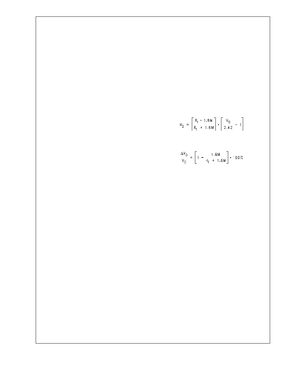
So proceeding in this manner, the worst-case resistive di-
vider equation (modified to include 1.6M
resistor in parallel
with R
1)is
Comparing this with the basic equation provides the follow-
ing error equation
Note that the right hand side depends on R
1 (not R2, nor the
output voltage directly). So for a given maximum allowed
error, first R
1 is calculated. Then the basic resistive divider
equation is invoked and used to calculate R
2.
The effect of R
1 is now considered.
If R
1 was say 5k, the error is about 0.3%. This error is in the
’+’ direction as mentioned earlier, for the case of current
flowing into the pin. The error is reduced to 0.14% for the
value R
1 = 2.21k as used in the Typical Application circuit. In
general it can be concluded that to restrict the error to within
0.25%, R
1should be 4k (or less).
If R
1 is 4.02k (a standard value), R2 as calculated from the
basic resistive divider design equation is 4.286k for a 5V
output and is 1.462k for a 3.3V output.
There is an alternative way of stating the error, in terms of
current rather than resistance. Since if R
1=4k, the current
flowing through the resistive divider is 2.42/4k=0.6mA, there-
fore it can also be stated that the divider current should be
0.6mA or less. This will restrict the error (due to the feedback
pin current and its variation) to less than 0.25%. This ’thum-
brule’ does not depend on input or output conditions, and is
typical for most applications.
The other related problem is that to get an exact value for R
1
or R
2 from standard resistor values may not be easy. Any
one of the two resistors can of course be selected to be a
standard value, but the other value as calculated from the
equation, will more likely than not, not correspond to any
standard value. The so called ’EIA standard values’ are the
E6, E12, E24, E48, E96 and E192 series, listed in most
resistor catalogs. E12 for example has 12 values in every
decade of resistance. The reader can for example do a
search within a typical vendor’s index home page e.g. http://
www.vishay.com/ with the keyword E96 for the table of stan-
dard values.
LM1572
www.national.com
14
相关PDF资料 |
PDF描述 |
|---|---|
| LM1572MTCX-5.0/NOPB | 3.2 A SWITCHING REGULATOR, 570 kHz SWITCHING FREQ-MAX, PDSO16 |
| LM1572MTCX-3.3/NOPB | 3.2 A SWITCHING REGULATOR, 570 kHz SWITCHING FREQ-MAX, PDSO16 |
| LM1572MTC-3.3/NOPB | 3.2 A SWITCHING REGULATOR, 570 kHz SWITCHING FREQ-MAX, PDSO16 |
| LM1572MTC-ADJ/NOPB | 3.2 A SWITCHING REGULATOR, 570 kHz SWITCHING FREQ-MAX, PDSO16 |
| LM1575J-ADJ/883 | 3 A SWITCHING REGULATOR, 58 kHz SWITCHING FREQ-MAX, CDIP16 |
相关代理商/技术参数 |
参数描述 |
|---|---|
| LM1575 | 制造商:NSC 制造商全称:National Semiconductor 功能描述:SIMPLE SWITCHER㈢ 1A Step-Down Voltage Regulator |
| LM1575_07 | 制造商:NSC 制造商全称:National Semiconductor 功能描述:SIMPLE SWITCHER㈢ 1A Step-Down Voltage Regulator |
| LM1575-12 | 制造商:NSC 制造商全称:National Semiconductor 功能描述:SIMPLE SWITCHER 1A STEP-DOWN VOLTAGE REGULATOR |
| LM1575-15 | 制造商:NSC 制造商全称:National Semiconductor 功能描述:SIMPLE SWITCHER(TM) 1A STEP-DOWN VOLTAGE REGULATOR |
| LM1575-5.0AK | 制造商:未知厂家 制造商全称:未知厂家 功能描述:Voltage-Mode SMPS Controller |
发布紧急采购,3分钟左右您将得到回复。