- 您现在的位置:买卖IC网 > PDF目录14440 > LM2574DW-ADJR2G (ON Semiconductor)IC REG BUCK ADJ 0.5A 16SOICW PDF资料下载
参数资料
| 型号: | LM2574DW-ADJR2G |
| 厂商: | ON Semiconductor |
| 文件页数: | 18/26页 |
| 文件大小: | 0K |
| 描述: | IC REG BUCK ADJ 0.5A 16SOICW |
| 标准包装: | 1,000 |
| 类型: | 降压(降压) |
| 输出类型: | 可调式 |
| 输出数: | 1 |
| 输出电压: | 1.23 V ~ 37 V |
| 输入电压: | 4.75 V ~ 40 V |
| PWM 型: | 电压模式 |
| 频率 - 开关: | 52kHz |
| 电流 - 输出: | 500mA |
| 同步整流器: | 无 |
| 工作温度: | -40°C ~ 125°C |
| 安装类型: | 表面贴装 |
| 封装/外壳: | 16-SOIC(0.295",7.50mm 宽) |
| 包装: | 带卷 (TR) |
| 供应商设备封装: | 16-SOIC W |
| 其它名称: | LM2574DW-ADJR2G-ND LM2574DW-ADJR2GOSTR |
�� �
�
�LM2574,� NCV2574�
�4.� R� q� JC�
�5.� R� q� JA�
�t�
�d� +� on� +� O� ,�
�in�
�Since� the� current� rating� of� the� LM2574� is� only� 0.5� A,� the�
�total� package� power� dissipation� for� this� switcher� is� quite�
�low,� ranging� from� approximately� 0.1� W� up� to� 0.75� W� under�
�varying� conditions.� In� a� carefully� engineered� printed� circuit�
�board,� the� through?hole� DIP� package� can� easily� dissipate� up�
�to� 0.75� W,� even� at� ambient� temperatures� of� 60� °� C,� and� still�
�keep� the� maximum� junction� temperature� below� 125� °� C.�
�Thermal� Analysis� and� Design�
�The� following� procedure� must� be� performed� to� determine�
�the� operating� junction� temperature.� First� determine:�
�1.� P� D(max)� ?� maximum� regulator� power� dissipation� in�
�the� application.�
�2.� T� A(max)� ?� maximum� ambient� temperature� in� the�
�application.�
�3.� T� J(max)� ?� maximum� allowed� junction� temperature�
�(125� °� C� for� the� LM2574).� For� a� conservative�
�design,� the� maximum� junction� temperature�
�should� not� exceed� 110� °� C� to� assure� safe�
�operation.� For� every� additional� +10� °� C�
�temperature� rise� that� the� junction� must�
�withstand,� the� estimated� operating� lifetime�
�of� the� component� is� halved.�
�?� package� thermal� resistance� junction?case.�
�?� package� thermal� resistance� junction?ambient.�
���The� following� formula� is� to� calculate� the� approximate�
�total� power� dissipated� by� the� LM2574:�
�P� D� =� (V� in� x� I� Q� )� +� d� x� I� Load� x� V� sat�
�where� d� is� the� duty� cycle� and� for� buck� converter�
�V�
�T� V�
�I� Q� (quiescent� current)� and� V� sat� can� be� found� in� the�
�LM2574� data� sheet,�
�V� in� is� minimum� input� voltage� applied,�
�V� O� is� the� regulator� output� voltage,�
�I� Load� is� the� load� current.�
�T� J� =� (R� q� JA� )(P� D� )� +� T� A�
�where� (R� q� JA� )(P� D� )� represents� the� junction� temperature� rise�
�caused� by� the� dissipated� power� and� T� A� is� the� maximum�
�ambient� temperature.�
�Some� Aspects� That� can� Influence� Thermal� Design�
�It� should� be� noted� that� the� package� thermal� resistance� and�
�the� junction� temperature� rise� numbers� are� all� approximate,�
�and� there� are� many� factors� that� will� affect� these� numbers,�
�such� as� PC� board� size,� shape,� thickness,� physical� position,�
�location,� board� temperature,� as� well� as� whether� the�
�surrounding� air� is� moving� or� still.� At� higher� power� levels� the�
�thermal� resistance� decreases� due� to� the� increased� air� current�
�activity.�
�Other� factors� are� trace� width,� total� printed� circuit� copper�
�area,� copper� thickness,� single?� or� double?sided,� multilayer�
�board,� the� amount� of� solder� on� the� board� or� even� color� of� the�
�traces.�
�The� size,� quantity� and� spacing� of� other� components� on� the�
�board� can� also� influence� its� effectiveness� to� dissipate� the�
�heat.� Some� of� them,� like� the� catch� diode� or� the� inductor� will�
�generate� some� additional� heat.�
�ADDITIONAL� APPLICATIONS�
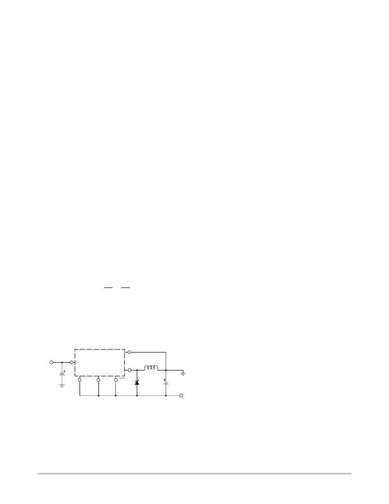
�Inverting� Regulator�
�An� inverting� buck?boost� regulator� using� the� LM2574?12�
�is� shown� in� Figure� 27.� This� circuit� converts� a� positive� input�
�voltage� to� a� negative� output� voltage� with� a� common� ground�
�by� bootstrapping� the� regulators� ground� to� the� negative�
�output� voltage.� By� grounding� the� feedback� pin,� the� regulator�
�senses� the� inverted� output� voltage� and� regulates� it.�
�In� this� example� the� LM2574?12� is� used� to� generate� a� ?12� V�
�output.� The� maximum� input� voltage� in� this� case� cannot�
�exceed� 28� V� because� the� maximum� voltage� appearing� across�
�the� regulator� is� the� absolute� sum� of� the� input� and� output�
�voltages� and� this� must� be� limited� to� a� maximum� of� 40� V.�
�This� circuit� configuration� is� able� to� deliver� approximately�
�0.1� A� to� the� output� when� the� input� voltage� is� 8.0� V� or� higher.�
�At� lighter� loads� the� minimum� input� voltage� required� drops�
�to� approximately� 4.7� V,� because� the� buck?boost� regulator�
�L1�
�(5)�
�8.0� to� 25� V�
�Unregulated�
�DC� Input� +V� in�
�5�
�C� in�
�22� m� F�
�4�
�LM2574?12�
�(12)�
�Pwr� 2� Sig� 3�
�Gnd� Gnd�
�(6)� (4)�
�(3)�
�(14)�
�Feedback�
�1�
�68� m� H�
�Output�
�7�
�ON/OFF� D1�
�MBR150�
�C� out�
�680� m� F�
�topology� can� produce� an� output� voltage� that,� in� its� absolute�
�value,� is� either� greater� or� less� than� the� input� voltage.�
�Since� the� switch� currents� in� this� buck?boost� configuration�
�are� higher� than� in� the� standard� buck� converter� topology,� the�
�available� output� current� is� lower.�
�This� type� of� buck?boost� inverting� regulator� can� also�
�require� a� larger� amount� of� startup� input� current,� even� for�
�?12� V� @� 100� mA�
�Regulated�
�Output�
�Figure� 27.� Inverting� Buck?Boost� Develops� ?12� V�
�The� dynamic� switching� losses� during� turn?on� and�
�turn?off� can� be� neglected� if� a� proper� type� catch� diode� is� used.�
�The� junction� temperature� can� be� determined� by� the�
�light� loads.� This� may� overload� an� input� power� source� with�
�a� current� limit� less� than� 0.6� A.�
�Because� of� the� relatively� high� startup� currents� required� by�
�this� inverting� regulator� topology,� the� use� of� a� delayed� startup�
�or� an� undervoltage� lockout� circuit� is� recommended.�
�While� using� a� delayed� startup� arrangement,� the� input�
�capacitor� can� charge� up� to� a� higher� voltage� before� the�
�switch?mode� regulator� begins� to� operate.�
�following� expression:�
�http://onsemi.com�
�18�
�相关PDF资料 |
PDF描述 |
|---|---|
| LM2574N-3.3G | IC REG BUCK 3.3V 0.5A 8DIP |
| LQG15HN12NJ02D | INDUCTOR 12NH 300MA 0402 |
| LM2574N-ADJG | IC REG BUCK ADJ 0.5A 8DIP |
| LM2574N-12G | IC REG BUCK 12V 0.5A 8DIP |
| LQG15HN10NJ02D | INDUCTOR 10NH 300MA 0402 |
相关代理商/技术参数 |
参数描述 |
|---|---|
| LM2574HV | 制造商:NSC 制造商全称:National Semiconductor 功能描述: |
| LM2574HVM-12 | 功能描述:直流/直流开关转换器 RoHS:否 制造商:STMicroelectronics 最大输入电压:4.5 V 开关频率:1.5 MHz 输出电压:4.6 V 输出电流:250 mA 输出端数量:2 最大工作温度:+ 85 C 安装风格:SMD/SMT |
| LM2574HVM-12/NOPB | 功能描述:直流/直流开关转换器 RoHS:否 制造商:STMicroelectronics 最大输入电压:4.5 V 开关频率:1.5 MHz 输出电压:4.6 V 输出电流:250 mA 输出端数量:2 最大工作温度:+ 85 C 安装风格:SMD/SMT |
| LM2574HVM-12/NOPB | 制造商:Texas Instruments 功能描述:DC/DC Converter IC |
| LM2574HVM-15 | 功能描述:直流/直流开关转换器 RoHS:否 制造商:STMicroelectronics 最大输入电压:4.5 V 开关频率:1.5 MHz 输出电压:4.6 V 输出电流:250 mA 输出端数量:2 最大工作温度:+ 85 C 安装风格:SMD/SMT |
发布紧急采购,3分钟左右您将得到回复。