- 您现在的位置:买卖IC网 > PDF目录149393 > LM2575T-005G (ON SEMICONDUCTOR) 3.2 A SWITCHING REGULATOR, 63 kHz SWITCHING FREQ-MAX, PSFM5 PDF资料下载
参数资料
| 型号: | LM2575T-005G |
| 厂商: | ON SEMICONDUCTOR |
| 元件分类: | 稳压器 |
| 英文描述: | 3.2 A SWITCHING REGULATOR, 63 kHz SWITCHING FREQ-MAX, PSFM5 |
| 封装: | LEAD FREE, TO-220, 5 PIN |
| 文件页数: | 10/29页 |
| 文件大小: | 408K |
| 代理商: | LM2575T-005G |
第1页第2页第3页第4页第5页第6页第7页第8页第9页当前第10页第11页第12页第13页第14页第15页第16页第17页第18页第19页第20页第21页第22页第23页第24页第25页第26页第27页第28页第29页
LM2575, NCV2575
http://onsemi.com
18
GENERAL RECOMMENDATIONS
Output Voltage Ripple and Transients
Source of the Output Ripple
Since the LM2575 is a switch mode power supply
regulator, its output voltage, if left unfiltered, will contain a
sawtooth ripple voltage at the switching frequency. The
output ripple voltage value ranges from 0.5% to 3% of the
output voltage. It is caused mainly by the inductor sawtooth
ripple current multiplied by the ESR of the output capacitor.
Short Voltage Spikes and How to Reduce Them
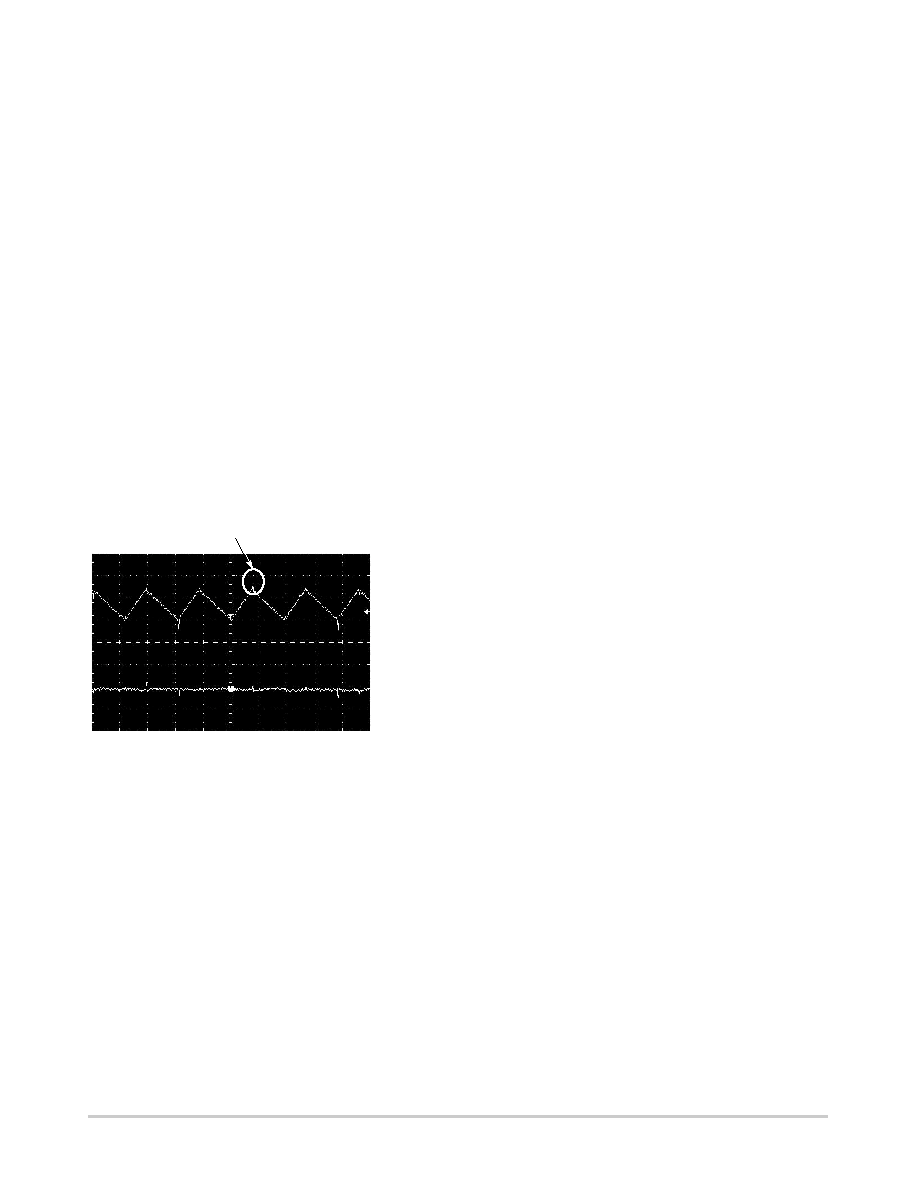
The regulator output voltage may also contain short
voltage spikes at the peaks of the sawtooth waveform (see
Figure 24). These voltage spikes are present because of the
fast switching action of the output switch, and the parasitic
inductance of the output filter capacitor. There are some
other important factors such as wiring inductance, stray
capacitance, as well as the scope probe used to evaluate these
transients, all these contribute to the amplitude of these
spikes. To minimize these voltage spikes, low inductance
capacitors should be used, and their lead lengths must be
kept short. The importance of quality printed circuit board
layout design should also be highlighted.
Figure 24. Output Ripple Voltage Waveforms
HORIZONTAL TIME BASE: 10
ms/DIV
UNFILTERED
OUTPUT
VOLTAGE
VERTICAL
RESOLUTION:
20 mV/DIV
FILTERED
OUTPUT
VOLTAGE
Voltage spikes caused by switching action of the output
switch and the parasitic inductance of the output capacitor
Minimizing the Output Ripple
In order to minimize the output ripple voltage it is possible
to enlarge the inductance value of the inductor L1 and/or to
use a larger value output capacitor. There is also another way
to smooth the output by means of an additional LC filter
(20
mH, 100 mF), that can be added to the output (see
Figure 33) to further reduce the amount of output ripple and
transients. With such a filter it is possible to reduce the
output ripple voltage transients 10 times or more. Figure 24
shows the difference between filtered and unfiltered output
waveforms of the regulator shown in Figure 33.
The upper waveform is from the normal unfiltered output
of the converter, while the lower waveform shows the output
ripple voltage filtered by an additional LC filter.
Heatsinking and Thermal Considerations
The ThroughHole Package TO220
The LM2575 is available in two packages, a 5pin
TO220(T, TV) and a 5pin surface mount D2PAK(D2T).
There are many applications that require no heatsink to keep
the LM2575 junction temperature within the allowed
operating range. The TO220 package can be used without
a heatsink for ambient temperatures up to approximately
50
°C (depending on the output voltage and load current).
Higher ambient temperatures require some heatsinking,
either to the printed circuit (PC) board or an external
heatsink.
The Surface Mount Package D2PAK and its
Heatsinking
The other type of package, the surface mount D2PAK, is
designed to be soldered to the copper on the PC board. The
copper and the board are the heatsink for this package and
the other heat producing components, such as the catch
diode and inductor. The PC board copper area that the
package is soldered to should be at least 0.4 in2 (or 100 mm2)
and ideally should have 2 or more square inches (1300 mm2)
of 0.0028 inch copper. Additional increasing of copper area
beyond approximately 3.0 in2 (2000 mm2) will not improve
heat dissipation significantly. If further thermal
improvements are needed, double sided or multilayer PC
boards with large copper areas should be considered.
Thermal Analysis and Design
The following procedure must be performed to determine
whether or not a heatsink will be required. First determine:
1. PD(max)
maximum regulator power dissipation in
the application.
2. TA(max)
maximum ambient temperature in the
application.
3. TJ(max)
maximum allowed junction temperature
(125
°C for the LM2575). For a conservative
design, the maximum junction temperature
should not exceed 110
°C to assure safe
operation. For every additional 10
°C
temperature rise that the junction must
withstand, the estimated operating lifetime
of the component is halved.
4. RqJC
package thermal resistance junctioncase.
5. RqJA
package thermal resistance junctionambient.
(Refer to Absolute Maximum Ratings in this data sheet or
RqJC and RqJA values).
The following formula is to calculate the total power
dissipated by the LM2575:
PD = (Vin x IQ) + d x ILoad x Vsat
where d is the duty cycle and for buck converter
相关PDF资料 |
PDF描述 |
|---|---|
| LK5320-9PD0TB1 | 2-OUTPUT 150 W AC-DC PWR FACTOR CORR MODULE |
| LS1501-9EPD0T | 1-OUTPUT 100 W AC-DC REG PWR SUPPLY MODULE |
| LS1501-9EPD1T | 1-OUTPUT 100 W AC-DC REG PWR SUPPLY MODULE |
| LS1501-9ERDDT | 1-OUTPUT 100 W AC-DC REG PWR SUPPLY MODULE |
| LS2320-7ERD7T | 2-OUTPUT 100 W AC-DC REG PWR SUPPLY MODULE |
相关代理商/技术参数 |
参数描述 |
|---|---|
| LM2575T-012 | 功能描述:直流/直流开关调节器 12V 1A Buck PWM RoHS:否 制造商:International Rectifier 最大输入电压:21 V 开关频率:1.5 MHz 输出电压:0.5 V to 0.86 V 输出电流:4 A 输出端数量: 最大工作温度: 安装风格:SMD/SMT 封装 / 箱体:PQFN 4 x 5 |
| LM2575T-012G | 功能描述:直流/直流开关转换器 12V 1A Buck PWM RoHS:否 制造商:STMicroelectronics 最大输入电压:4.5 V 开关频率:1.5 MHz 输出电压:4.6 V 输出电流:250 mA 输出端数量:2 最大工作温度:+ 85 C 安装风格:SMD/SMT |
| LM2575T-015 | 功能描述:直流/直流开关调节器 15V 1A Buck PWM RoHS:否 制造商:International Rectifier 最大输入电压:21 V 开关频率:1.5 MHz 输出电压:0.5 V to 0.86 V 输出电流:4 A 输出端数量: 最大工作温度: 安装风格:SMD/SMT 封装 / 箱体:PQFN 4 x 5 |
| LM2575T-015G | 制造商:ONSEMI 制造商全称:ON Semiconductor 功能描述:1.0 A, Adjustable Output Voltage, Step−Down Switching Regulator |
| LM2575T12 | 制造商:Semtech 功能描述:_ |
发布紧急采购,3分钟左右您将得到回复。