- 您现在的位置:买卖IC网 > PDF目录149393 > LM2575T-005G (ON SEMICONDUCTOR) 3.2 A SWITCHING REGULATOR, 63 kHz SWITCHING FREQ-MAX, PSFM5 PDF资料下载
参数资料
| 型号: | LM2575T-005G |
| 厂商: | ON SEMICONDUCTOR |
| 元件分类: | 稳压器 |
| 英文描述: | 3.2 A SWITCHING REGULATOR, 63 kHz SWITCHING FREQ-MAX, PSFM5 |
| 封装: | LEAD FREE, TO-220, 5 PIN |
| 文件页数: | 13/29页 |
| 文件大小: | 408K |
| 代理商: | LM2575T-005G |
第1页第2页第3页第4页第5页第6页第7页第8页第9页第10页第11页第12页当前第13页第14页第15页第16页第17页第18页第19页第20页第21页第22页第23页第24页第25页第26页第27页第28页第29页
LM2575, NCV2575
http://onsemi.com
20
Using a delayed startup arrangement, the input capacitor
can charge up to a higher voltage before the switchmode
regulator begins to operate.
The high input current needed for startup is now partially
supplied by the input capacitor Cin.
Design Recommendations:
The inverting regulator operates in a different manner
than the buck converter and so a different design procedure
has to be used to select the inductor L1 or the output
capacitor Cout.
The output capacitor values must be larger than is
normally required for buck converter designs. Low input
voltages or high output currents require a large value output
capacitor (in the range of thousands of
mF).
The recommended range of inductor values for the
inverting converter design is between 68
mH and 220 mH. To
select an inductor with an appropriate current rating, the
inductor peak current has to be calculated.
The following formula is used to obtain the peak inductor
current:
where ton +
|VO|
Vin ) |VO|
x 1
fosc
, and fosc + 52 kHz.
Ipeak [
ILoad (Vin ) |VO|)
Vin
)
Vin xton
2L1
Under normal continuous inductor current operating
conditions, the worst case occurs when Vin is minimal.
Note that the voltage appearing across the regulator is the
absolute sum of the input and output voltage, and must not
exceed 40 V.
Figure 26. Inverting BuckBoost
Regulator with Delayed Startup
D1
1N5819
L1
100
mH
Output
2
4
Feedback
Unregulated
DC Input
12 V to 25 V
Cin
100
mF
/50 V
1
3
5ON/OFF
GND
+Vin
Regulated
Output
-12 V @ 0.35 A
Cout
1800
mF
/16 V
LM257512
C1
0.1
mF
R1
47 k
R2
47 k
It has been already mentioned above, that in some
situations, the delayed startup or the undervoltage lockout
features could be very useful. A delayed startup circuit
applied to a buckboost converter is shown in Figure 26.
Figure 32 in the “Undervoltage Lockout” section describes
an undervoltage lockout feature for the same converter
topology.
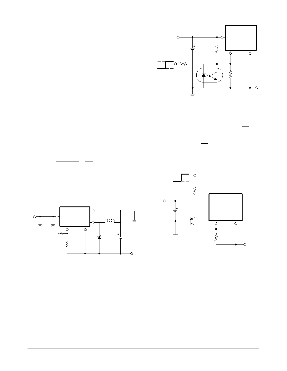
Figure 27. Inverting BuckBoost Regulator Shut Down
Circuit Using an Optocoupler
LM2575XX
1
3
5
GND
ON/OFF
+Vin
R2
47 k
Cin
100
mF
NOTE: This picture does not show the complete circuit.
R1
47 k
R3
470
Shutdown
Input
MOC8101
-Vout
Off
On
5.0 V
0
+Vin
With the inverting configuration, the use of the ON/OFF
pin requires some level shifting techniques. This is caused
by the fact, that the ground pin of the converter IC is no
longer at ground. Now, the ON/OFF pin threshold voltage
(1.4 V approximately) has to be related to the negative
output voltage level. There are many different possible shut
Figure 28. Inverting BuckBoost Regulator Shut Down
Circuit Using a PNP Transistor
NOTE: This picture does not show the complete circuit.
R2
5.6 k
Q1
2N3906
LM2575XX
1
3
5
GND
ON/OFF
R1
12 k
-Vout
+Vin
Shutdown
Input
Off
On
+V
0
+Vin
Cin
100
mF
Negative Boost Regulator
This example is a variation of the buckboost topology
and is called a negative boost regulator. This regulator
experiences relatively high switch current, especially at low
input voltages. The internal switch current limiting results in
lower output load current capability.
The circuit in Figure 29 shows the negative boost
configuration. The input voltage in this application ranges
from 5.0 V to 12 V and provides a regulated 12 V output.
相关PDF资料 |
PDF描述 |
|---|---|
| LK5320-9PD0TB1 | 2-OUTPUT 150 W AC-DC PWR FACTOR CORR MODULE |
| LS1501-9EPD0T | 1-OUTPUT 100 W AC-DC REG PWR SUPPLY MODULE |
| LS1501-9EPD1T | 1-OUTPUT 100 W AC-DC REG PWR SUPPLY MODULE |
| LS1501-9ERDDT | 1-OUTPUT 100 W AC-DC REG PWR SUPPLY MODULE |
| LS2320-7ERD7T | 2-OUTPUT 100 W AC-DC REG PWR SUPPLY MODULE |
相关代理商/技术参数 |
参数描述 |
|---|---|
| LM2575T-012 | 功能描述:直流/直流开关调节器 12V 1A Buck PWM RoHS:否 制造商:International Rectifier 最大输入电压:21 V 开关频率:1.5 MHz 输出电压:0.5 V to 0.86 V 输出电流:4 A 输出端数量: 最大工作温度: 安装风格:SMD/SMT 封装 / 箱体:PQFN 4 x 5 |
| LM2575T-012G | 功能描述:直流/直流开关转换器 12V 1A Buck PWM RoHS:否 制造商:STMicroelectronics 最大输入电压:4.5 V 开关频率:1.5 MHz 输出电压:4.6 V 输出电流:250 mA 输出端数量:2 最大工作温度:+ 85 C 安装风格:SMD/SMT |
| LM2575T-015 | 功能描述:直流/直流开关调节器 15V 1A Buck PWM RoHS:否 制造商:International Rectifier 最大输入电压:21 V 开关频率:1.5 MHz 输出电压:0.5 V to 0.86 V 输出电流:4 A 输出端数量: 最大工作温度: 安装风格:SMD/SMT 封装 / 箱体:PQFN 4 x 5 |
| LM2575T-015G | 制造商:ONSEMI 制造商全称:ON Semiconductor 功能描述:1.0 A, Adjustable Output Voltage, Step−Down Switching Regulator |
| LM2575T12 | 制造商:Semtech 功能描述:_ |
发布紧急采购,3分钟左右您将得到回复。