- 您现在的位置:买卖IC网 > PDF目录44548 > LM2586SX-12/NOPB (NATIONAL SEMICONDUCTOR CORP) 3 A SWITCHING REGULATOR, 200 kHz SWITCHING FREQ-MAX, PSSO7 PDF资料下载
参数资料
| 型号: | LM2586SX-12/NOPB |
| 厂商: | NATIONAL SEMICONDUCTOR CORP |
| 元件分类: | 稳压器 |
| 英文描述: | 3 A SWITCHING REGULATOR, 200 kHz SWITCHING FREQ-MAX, PSSO7 |
| 封装: | TO-263, 7 PIN |
| 文件页数: | 19/30页 |
| 文件大小: | 1273K |
| 代理商: | LM2586SX-12/NOPB |
第1页第2页第3页第4页第5页第6页第7页第8页第9页第10页第11页第12页第13页第14页第15页第16页第17页第18页当前第19页第20页第21页第22页第23页第24页第25页第26页第27页第28页第29页第30页
Application Hints (Continued)
with an external current limit circuit. The external limit should
be set to the maximum switch current of the device, which is
3A.
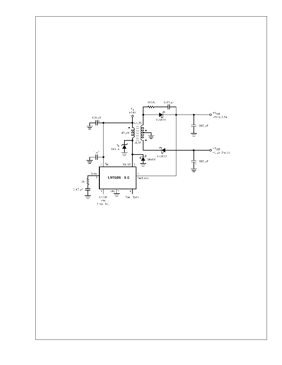
In a flyback regulator application (Figure 43), using the stan-
dard transformers, the LM2586 will survive a short circuit to
the main output. When the output voltage drops to 80% of its
nominal value, the frequency will drop to 25 kHz. With a
lower frequency, off times are larger. With the longer off
times, the transformer can release all of its stored energy
before the switch turns back on. Hence, the switch turns on
initially with zero current at its collector. In this condition, the
switch current limit will limit the peak current, saving the
device.
FLYBACK REGULATOR INPUT CAPACITORS
A flyback regulator draws discontinuous pulses of current
from the input supply. Therefore, there are two input capaci-
tors needed in a flyback regulator — one for energy storage
and one for filtering (see Figure 43). Both are required due to
the inherent operation of a flyback regulator. To keep a
stable or constant voltage supply to the LM2586, a storage
capacitor (
≥100 F) is required. If the input source is a
rectified DC supply and/or the application has a wide tem-
perature range, the required rms current rating of the capaci-
tor might be very large. This means a larger value of capaci-
tance or a higher voltage rating will be needed for the input
capacitor. The storage capacitor will also attenuate noise
which may interfere with other circuits connected to the
same input supply voltage.
In addition, a small bypass capacitor is required due to the
noise generated by the input current pulses. To eliminate the
noise, insert a 1.0 F ceramic capacitor between V
IN and
ground as close as possible to the device.
SWITCH VOLTAGE LIMITS
In a flyback regulator, the maximum steady-state voltage
appearing at the switch, when it is off, is set by the trans-
former turns ratio, N, the output voltage, V
OUT, and the
maximum input voltage, V
IN (Max):
V
SW(OFF) =VIN (Max) + (VOUT +VF)/N
where V
F is the forward biased voltage of the output diode,
and is typically 0.5V for Schottky diodes and 0.8V for ultra-
fast recovery diodes. In certain circuits, there exists a volt-
age spike, V
LL, superimposed on top of the steady-state
voltage (see Figure 5, waveform A). Usually, this voltage
spike is caused by the transformer leakage inductance
and/or the output rectifier recovery time. To “clamp” the
voltage at the switch from exceeding its maximum value, a
transient suppressor in series with a diode is inserted across
the transformer primary (as shown in the circuit in Figure 4
and
other
flyback
regulator
circuits
throughout
the
datasheet). The schematic in Figure 43 shows another
method of clamping the switch voltage. A single voltage
transient suppressor (the SA51A) is inserted at the switch
pin. This method clamps the total voltage across the switch,
not just the voltage across the primary.
If poor circuit layout techniques are used (see the “Circuit
Layout Guideline” section), negative voltage transients may
appear on the Switch pin (pin 5). Applying a negative voltage
(with respect to the IC’s ground) to any monolithic IC pin
causes erratic and unpredictable operation of that IC. This
holds true for the LM2586 IC as well. When used in a flyback
regulator, the voltage at the Switch pin (pin 5) can go nega-
tive when the switch turns on. The “ringing” voltage at the
switch pin is caused by the output diode capacitance and the
transformer leakage inductance forming a resonant circuit at
the secondary(ies). The resonant circuit generates the “ring-
ing” voltage, which gets reflected back through the trans-
former to the switch pin. There are two common methods to
avoid this problem. One is to add an RC snubber around the
output rectifier(s), as in Figure 43. The values of the resistor
and the capacitor must be chosen so that the voltage at the
Switch pin does not drop below 0.4V. The resistor may
01251662
FIGURE 43. Flyback Regulator
LM2586
www.national.com
26
相关PDF资料 |
PDF描述 |
|---|---|
| LM2587SX-3.3/NOPB | 5 A SWITCHING REGULATOR, 100 kHz SWITCHING FREQ-MAX, PSSO5 |
| LM2588-12MWC | 9.5 A SWITCHING REGULATOR, 200 kHz SWITCHING FREQ-MAX, UUC |
| LM2588-12MDC | 9.5 A SWITCHING REGULATOR, 200 kHz SWITCHING FREQ-MAX, UUC |
| LM2588-ADJMWC | 9.5 A SWITCHING REGULATOR, 200 kHz SWITCHING FREQ-MAX, UUC |
| LM2588T-12/NOPB | 9.5 A SWITCHING REGULATOR, 200 kHz SWITCHING FREQ-MAX, PSFM7 |
相关代理商/技术参数 |
参数描述 |
|---|---|
| LM2586SX-3.3 | 功能描述:直流/直流开关转换器 RoHS:否 制造商:STMicroelectronics 最大输入电压:4.5 V 开关频率:1.5 MHz 输出电压:4.6 V 输出电流:250 mA 输出端数量:2 最大工作温度:+ 85 C 安装风格:SMD/SMT |
| LM2586SX-3.3/NOPB | 功能描述:直流/直流开关转换器 RoHS:否 制造商:STMicroelectronics 最大输入电压:4.5 V 开关频率:1.5 MHz 输出电压:4.6 V 输出电流:250 mA 输出端数量:2 最大工作温度:+ 85 C 安装风格:SMD/SMT |
| LM2586SX-5.0 | 功能描述:直流/直流开关转换器 RoHS:否 制造商:STMicroelectronics 最大输入电压:4.5 V 开关频率:1.5 MHz 输出电压:4.6 V 输出电流:250 mA 输出端数量:2 最大工作温度:+ 85 C 安装风格:SMD/SMT |
| LM2586SX-5.0/NOPB | 功能描述:直流/直流开关转换器 RoHS:否 制造商:STMicroelectronics 最大输入电压:4.5 V 开关频率:1.5 MHz 输出电压:4.6 V 输出电流:250 mA 输出端数量:2 最大工作温度:+ 85 C 安装风格:SMD/SMT |
| LM2586SX-ADJ | 功能描述:直流/直流开关转换器 RoHS:否 制造商:STMicroelectronics 最大输入电压:4.5 V 开关频率:1.5 MHz 输出电压:4.6 V 输出电流:250 mA 输出端数量:2 最大工作温度:+ 85 C 安装风格:SMD/SMT |
发布紧急采购,3分钟左右您将得到回复。