- 您现在的位置:买卖IC网 > PDF目录44548 > LM2586SX-12/NOPB (NATIONAL SEMICONDUCTOR CORP) 3 A SWITCHING REGULATOR, 200 kHz SWITCHING FREQ-MAX, PSSO7 PDF资料下载
参数资料
| 型号: | LM2586SX-12/NOPB |
| 厂商: | NATIONAL SEMICONDUCTOR CORP |
| 元件分类: | 稳压器 |
| 英文描述: | 3 A SWITCHING REGULATOR, 200 kHz SWITCHING FREQ-MAX, PSSO7 |
| 封装: | TO-263, 7 PIN |
| 文件页数: | 27/30页 |
| 文件大小: | 1273K |
| 代理商: | LM2586SX-12/NOPB |
第1页第2页第3页第4页第5页第6页第7页第8页第9页第10页第11页第12页第13页第14页第15页第16页第17页第18页第19页第20页第21页第22页第23页第24页第25页第26页当前第27页第28页第29页第30页
Electrical Characteristics (Continued)
LM2586-ADJ (Continued)
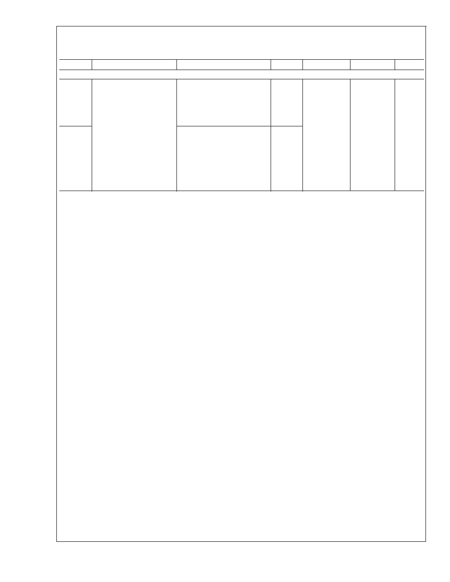
Symbol
Parameters
Conditions
Typical
Min
Max
Units
COMMON DEVICE PARAMETERS for all versions (Note 5)
θ
JA
Thermal Resistance
T Package, Junction to Ambient
65
C/W
θ
JA
T Package, Junction to Ambient
45
θ
JC
T Package, Junction to Case
2
θ
JA
S Package, Junction to Ambient
56
θ
JA
S Package, Junction to Ambient
35
θ
JA
S Package, Junction to Ambient
26
θ
JC
S Package, Junction to Case
2
Note 1: Absolute Maximum Ratings indicate limits beyond which damage to the device may occur. These ratings apply when the current is limited to less than
1.2 mA for pins 1, 2, 3, and 6. Operating ratings indicate conditions for which the device is intended to be functional, but device parameter specifications may not
be guaranteed under these conditions. For guaranteed specifications and test conditions, see the Electrical Characteristics.
Note 2: Note that switch current and output current are not identical in a step-up regulator. Output current cannot be internally limited when the LM2586 is used as
a step-up regulator. To prevent damage to the switch, the output current must be externally limited to 3A. However, output current is internally limited when the
LM2586 is used as a flyback regulator (see the Application Hints section for more information).
Note 3: The junction temperature of the device (TJ) is a function of the ambient temperature (TA), the junction-to-ambient thermal resistance (θJA), and the power
dissipation of the device (PD). A thermal shutdown will occur if the temperature exceeds the maximum junction temperature of the device: PD x θJA +TA(MAX) ≥
TJ(MAX). For a safe thermal design, check that the maximum power dissipated by the device is less than: PD ≤ [TJ(MAX) TA(MAX)]/θJA. When calculating the
maximum allowable power dissipation, derate the maximum junction temperature — this ensures a margin of safety in the thermal design.
Note 4: External components such as the diode, inductor, input and output capacitors can affect switching regulator performance. When the LM2586 is used as
shown in Figures 1, 2, system performance will be as specified by the system parameters.
Note 5: All room temperature limits are 100% production tested, and all limits at temperature extremes are guaranteed via correlation using standard Statistical
Quality Control (SQC) methods.
Note 6: A 1.0 M
resistor is connected to the compensation pin (which is the error amplifier output) to ensure accuracy in measuring AVOL.
Note 7: To measure this parameter, the feedback voltage is set to a low value, depending on the output version of the device, to force the error amplifier output high
and the switch on.
Note 8: To measure this parameter, the feedback voltage is set to a high value, depending on the output version of the device, to force the error amplifier output
low and the switch off.
Note 9: To measure the worst-case error amplifier output current, the LM2586 is tested with the feedback voltage set to its low value (Note 7) and at its high value
Note 10: When testing the minimum value, do not sink current from this pin — isolate it with a diode. If current is drawn from this pin, the frequency adjust circuit
will begin operation (see Figure 41).
Note 11: Junction to ambient thermal resistance (no external heat sink) for the 7 lead TO-220 package mounted vertically, with 12 inch leads in a socket, or on a
PC board with minimum copper area.
Note 12: Junction to ambient thermal resistance (no external heat sink) for the 7 lead TO-220 package mounted vertically, with 12 inch leads soldered to a PC board
containing approximately 4 square inches of (1 oz.) copper area surrounding the leads.
Note 13: Junction to ambient thermal resistance for the 7 lead TO-263 mounted horizontally against a PC board area of 0.136 square inches (the same size as the
TO-263 package) of 1 oz. (0.0014 in. thick) copper.
Note 14: Junction to ambient thermal resistance for the 7 lead TO-263 mounted horizontally against a PC board area of 0.4896 square inches (3.6 times the area
of the TO-263 package) of 1 oz. (0.0014 in. thick) copper.
Note 15: Junction to ambient thermal resistance for the 7 lead TO-263 mounted horizontally against a PC board copper area of 1.0064 square inches (7.4 times
the area of the TO-263 package) of 1 oz. (0.0014 in. thick) copper. Additional copper area will reduce thermal resistance further. See the thermal modelin Switchers
Made Simple software.
LM2586
www.national.com
6
相关PDF资料 |
PDF描述 |
|---|---|
| LM2587SX-3.3/NOPB | 5 A SWITCHING REGULATOR, 100 kHz SWITCHING FREQ-MAX, PSSO5 |
| LM2588-12MWC | 9.5 A SWITCHING REGULATOR, 200 kHz SWITCHING FREQ-MAX, UUC |
| LM2588-12MDC | 9.5 A SWITCHING REGULATOR, 200 kHz SWITCHING FREQ-MAX, UUC |
| LM2588-ADJMWC | 9.5 A SWITCHING REGULATOR, 200 kHz SWITCHING FREQ-MAX, UUC |
| LM2588T-12/NOPB | 9.5 A SWITCHING REGULATOR, 200 kHz SWITCHING FREQ-MAX, PSFM7 |
相关代理商/技术参数 |
参数描述 |
|---|---|
| LM2586SX-3.3 | 功能描述:直流/直流开关转换器 RoHS:否 制造商:STMicroelectronics 最大输入电压:4.5 V 开关频率:1.5 MHz 输出电压:4.6 V 输出电流:250 mA 输出端数量:2 最大工作温度:+ 85 C 安装风格:SMD/SMT |
| LM2586SX-3.3/NOPB | 功能描述:直流/直流开关转换器 RoHS:否 制造商:STMicroelectronics 最大输入电压:4.5 V 开关频率:1.5 MHz 输出电压:4.6 V 输出电流:250 mA 输出端数量:2 最大工作温度:+ 85 C 安装风格:SMD/SMT |
| LM2586SX-5.0 | 功能描述:直流/直流开关转换器 RoHS:否 制造商:STMicroelectronics 最大输入电压:4.5 V 开关频率:1.5 MHz 输出电压:4.6 V 输出电流:250 mA 输出端数量:2 最大工作温度:+ 85 C 安装风格:SMD/SMT |
| LM2586SX-5.0/NOPB | 功能描述:直流/直流开关转换器 RoHS:否 制造商:STMicroelectronics 最大输入电压:4.5 V 开关频率:1.5 MHz 输出电压:4.6 V 输出电流:250 mA 输出端数量:2 最大工作温度:+ 85 C 安装风格:SMD/SMT |
| LM2586SX-ADJ | 功能描述:直流/直流开关转换器 RoHS:否 制造商:STMicroelectronics 最大输入电压:4.5 V 开关频率:1.5 MHz 输出电压:4.6 V 输出电流:250 mA 输出端数量:2 最大工作温度:+ 85 C 安装风格:SMD/SMT |
发布紧急采购,3分钟左右您将得到回复。