- 您现在的位置:买卖IC网 > PDF目录44549 > LM2590HV3.3MDC (NATIONAL SEMICONDUCTOR CORP) 3 A SWITCHING REGULATOR, 173 kHz SWITCHING FREQ-MAX, UUC PDF资料下载
参数资料
| 型号: | LM2590HV3.3MDC |
| 厂商: | NATIONAL SEMICONDUCTOR CORP |
| 元件分类: | 稳压器 |
| 英文描述: | 3 A SWITCHING REGULATOR, 173 kHz SWITCHING FREQ-MAX, UUC |
| 封装: | DIE |
| 文件页数: | 9/24页 |
| 文件大小: | 816K |
| 代理商: | LM2590HV3.3MDC |
Application Information (Continued)
suming 100% efficiency, which is never so. Therefore expect
I
PEAK to be an additional 10-20% higher than calculated from
the above equation.
The reader is also referred to Application Note AN-1157 for
examples based on positive to negative configuration.
The maximum voltage appearing across the regulator is the
absolute sum of the input and output voltage, and this must
be limited to a maximum of 60V. In this example, when
converting +20V to 5V, the regulator would see 25V be-
tween the input pin and ground pin. The LM2590HV has a
maximum input voltage rating of 60V.
An additional diode is required in this regulator configuration.
Diode D1 is used to isolate input voltage ripple or noise from
coupling through the C
IN capacitor to the output, under light
or no load conditions. Also, this diode isolation changes the
topology to closely resemble a buck configuration thus pro-
viding good closed loop stability. A Schottky diode is recom-
mended for low input voltages, (because of its lower voltage
drop) but for higher input voltages, a IN5400 diode could be
used.
Because of differences in the operation of the inverting
regulator, the standard design procedure is not used to
select the inductor value. In the majority of designs, a 33 H,
3A inductor is the best choice. Capacitor selection can also
be narrowed down to just a few values.
This type of inverting regulator can require relatively large
amounts of input current when starting up, even with light
loads. Input currents as high as the LM2590HV current limit
(approximately 3.0A) are needed for 2 ms or more, until the
output reaches its nominal output voltage. The actual time
depends on the output voltage and the size of the output
capacitor. Input power sources that are current limited or
sources that can not deliver these currents without getting
loaded down, may not work correctly. Because of the rela-
tively high startup currents required by the inverting topology,
the Soft-Start feature shown in
Figure 10 is recommended.
Also shown in
Figure 10 are several shutdown methods for
the inverting configuration. With the inverting configuration,
some level shifting is required, because the ground pin of the
regulator is no longer at ground, but is now at the negative
output voltage. The shutdown methods shown accept
ground referenced shutdown signals.
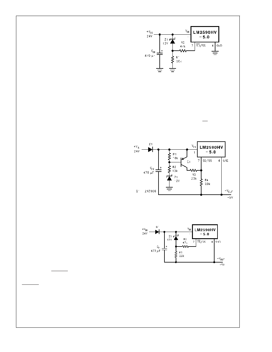
UNDERVOLTAGE LOCKOUT
Some applications require the regulator to remain off until
the input voltage reaches a predetermined voltage.
contains a undervoltage lockout circuit for a buck configura-
tion, while
(only the circuitry pertaining to the undervoltage lockout is
shown).
Figure 11 uses a zener diode to establish the
threshold voltage when the switcher begins operating. When
the input voltage is less than the zener voltage, resistors R1
and R2 hold the Shutdown /Soft-start pin low, keeping the
regulator in the shutdown mode. As the input voltage ex-
ceeds the zener voltage, the zener conducts, pulling the
Shutdown /Soft-start pin high, allowing the regulator to begin
switching. The threshold voltage for the undervoltage lockout
feature is approximately 1.5V greater than the zener voltage.
inverting circuit.
Figure 12 features a constant threshold
voltage for turn on and turn off (zener voltage plus approxi-
mately one volt). If hysteresis is needed, the circuit in
13 has a turn ON voltage which is different than the turn OFF
voltage. The amount of hysteresis is approximately equal to
the value of the output voltage. Since the SD /SS pin has an
internal 7V zener clamp, R2 is needed to limit the current into
this pin to approximately 1 mA when Q1 is on.
Layout Suggestions
As in any switching regulator, layout is very important. Rap-
idly switching currents associated with wiring inductance can
generate voltage transients which can cause problems. For
minimal inductance and ground loops, with reference to
Figure 1, the wires indicated by heavy lines should be wide
printed circuit traces and should be kept as short as
10134745
FIGURE 11. Undervoltage Lockout for a Buck
Regulator
10134747
FIGURE 12. Undervoltage Lockout Without
Hysteresis for an Inverting Regulator
10134746
FIGURE 13. Undervoltage Lockout With
Hysteresis for an Inverting Regulator
LM2590HV
www.national.com
17
相关PDF资料 |
PDF描述 |
|---|---|
| LM2594-12MDC | 1.4 A SWITCHING REGULATOR, 173 kHz SWITCHING FREQ-MAX, UUC |
| LM2594-5.0MWC | 1.4 A SWITCHING REGULATOR, 173 kHz SWITCHING FREQ-MAX, UUC |
| LM2594-ADJMDC | 1.4 A SWITCHING REGULATOR, 173 kHz SWITCHING FREQ-MAX, UUC |
| LM2594-ADJMWC | 1.4 A SWITCHING REGULATOR, 173 kHz SWITCHING FREQ-MAX, UUC |
| LM2594HV-12MWC | 1.4 A SWITCHING REGULATOR, 173 kHz SWITCHING FREQ-MAX, UUC |
相关代理商/技术参数 |
参数描述 |
|---|---|
| LM2590HVS-3.3 | 功能描述:直流/直流开关转换器 RoHS:否 制造商:STMicroelectronics 最大输入电压:4.5 V 开关频率:1.5 MHz 输出电压:4.6 V 输出电流:250 mA 输出端数量:2 最大工作温度:+ 85 C 安装风格:SMD/SMT |
| LM2590HVS-3.3/NOPB | 功能描述:直流/直流开关转换器 RoHS:否 制造商:STMicroelectronics 最大输入电压:4.5 V 开关频率:1.5 MHz 输出电压:4.6 V 输出电流:250 mA 输出端数量:2 最大工作温度:+ 85 C 安装风格:SMD/SMT |
| LM2590HVS-5.0 | 功能描述:直流/直流开关转换器 RoHS:否 制造商:STMicroelectronics 最大输入电压:4.5 V 开关频率:1.5 MHz 输出电压:4.6 V 输出电流:250 mA 输出端数量:2 最大工作温度:+ 85 C 安装风格:SMD/SMT |
| LM2590HVS5.0/NOPB | 制造商:Texas Instruments 功能描述: |
| LM2590HVS-5.0/NOPB | 功能描述:直流/直流开关转换器 RoHS:否 制造商:STMicroelectronics 最大输入电压:4.5 V 开关频率:1.5 MHz 输出电压:4.6 V 输出电流:250 mA 输出端数量:2 最大工作温度:+ 85 C 安装风格:SMD/SMT |
发布紧急采购,3分钟左右您将得到回复。