- 您现在的位置:买卖IC网 > PDF目录44549 > LM2637M/NOPB (NATIONAL SEMICONDUCTOR CORP) SWITCHING CONTROLLER, 1000 kHz SWITCHING FREQ-MAX, PDSO24 PDF资料下载
参数资料
| 型号: | LM2637M/NOPB |
| 厂商: | NATIONAL SEMICONDUCTOR CORP |
| 元件分类: | 稳压器 |
| 英文描述: | SWITCHING CONTROLLER, 1000 kHz SWITCHING FREQ-MAX, PDSO24 |
| 封装: | SOIC-24 |
| 文件页数: | 2/17页 |
| 文件大小: | 803K |
| 代理商: | LM2637M/NOPB |
Applications Information (Continued)
happens, the error in the output voltage level is fed to the
error amplifier. The output of the error amplifier is then
compared with an internally generated PWM ramp signal
and the result of the comparison is a series of pulses with
certain duty ratios. These pulses are then used to control the
on and off of the FET gate drives. In this way, the error in the
output voltage gets corrected by the change in the duty ratio
of the FET switches. During a large load transient, depend-
ing on the compensation design, the change in duty ratio
usually begins within one switching cycle. Refer to the De-
sign Considerations section for more details.
Besides the voltage feedback control loop, the LM2637 also
has a pair of fast comparators (the MIN and MAX compara-
tors) to help maintain the output voltage during a large and
fast load transient. The trip points of the comparators are set
to ±5% of the DAC output voltage. When the load transient
is so large that the output voltage goes outside the ±5%
window, the MIN or MAX comparator will bypass the primary
voltage control loop and immediately set the duty ratio to
either 100% or 0%. This provides the fastest possible way to
react to such a large load transient in a conventional buck
converter.
Linear Section — The linear section has a high control band-
width. Depending on external components selected, the typi-
cal bandwidth can be as high as 1.2 MHz. The user may
choose to lower this bandwidth and have a better noise
immunity by adding a small capacitor (1 nF to 10 nF) be-
tween the gate output and ground.
Power Good Signal
The power good signal is to indicate whether all three output
voltages are within their corresponding range. The range for
the switching regulator is set to a typical ±10% window of the
DAC output voltage. The range for the linear regulator is
0.63V to infinity. During soft start, the power good signal is
kept low. At the completion of soft start, all three output
voltages are checked and the PWGD pin will be asserted if
they are all within specified range. During normal operation,
whenever a voltage goes out of the specified range for more
than about 3 s, PWGD pin will be pulled low.
Over-Voltage Protection
Switching Section — When the output voltage exceeds 118%
of the DAC output voltage any time beyond the soft start, the
switching section will enter over-voltage protection mode
and shuts itself down. The upper gate drive will be held low
while the lower gate drive will be held high. PWGD will be
low. There will also be a logic high signal at the OVP pin that
can be used to fire an external SCR. To clear this mode, refer
to the Resetting the LM2637 section.
Linear Section — There is no over-voltage protection in the
linear controllers.
Under-Voltage Latch-Off
At the completion of soft start, the controller starts to monitor
all three output voltages. If any of the voltages goes below
about 0.63V, the controller will latch off its corresponding
section, i.e., switching or linear. The mode can be cleared by
following the procedures described in the Resetting the
LM2637 section.
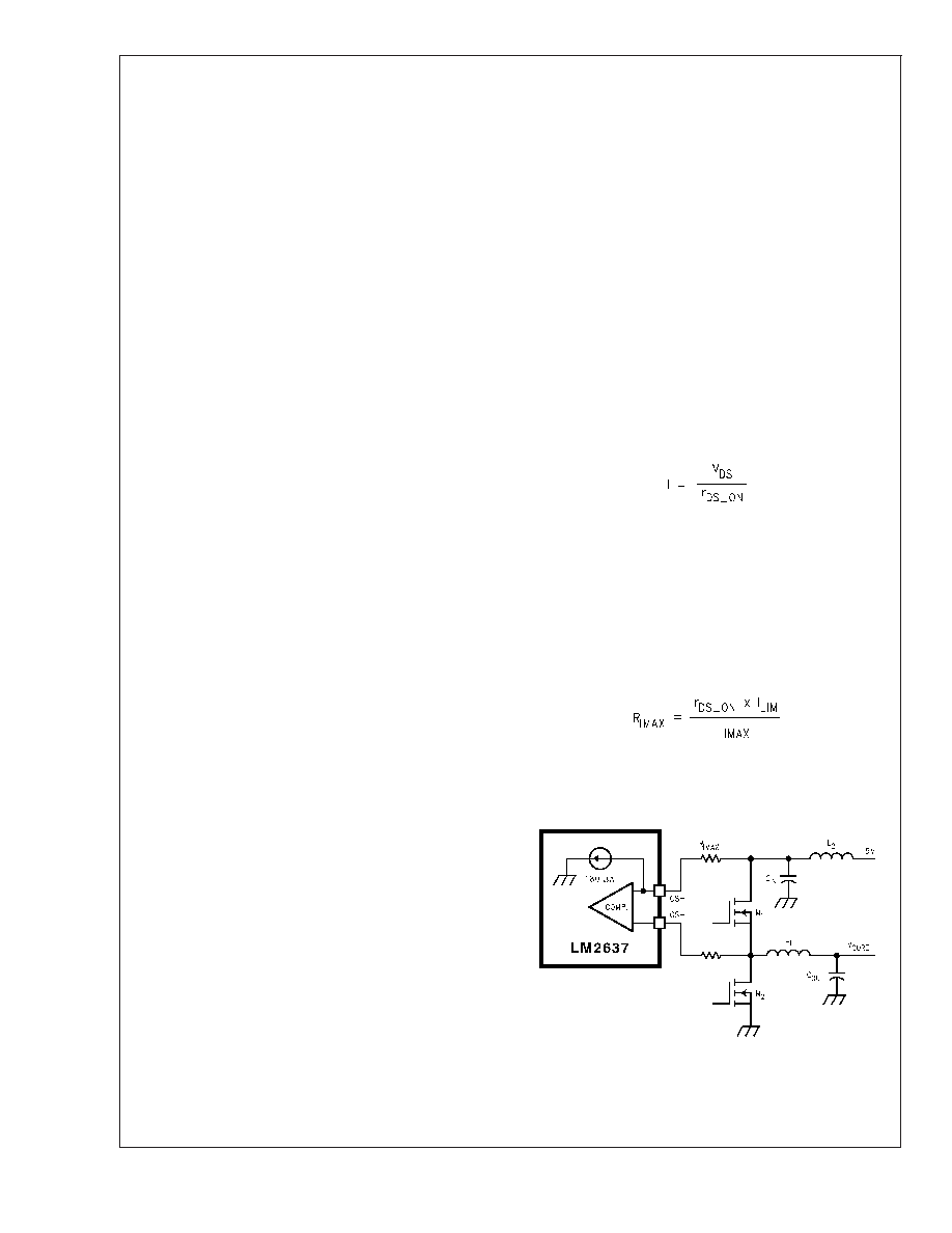
Current Limit
Switching Section — Current limit can be realized by two
methods. One method is through sensing the V
DS of the
high-side FET. The other is through a separate sense resis-
tor. The first method is cheaper and more power efficient but
less accurate. The second method is more accurate but
dissipates additional power and is either more expensive or
requires special PCB layout consideration. A side benefit of
the second method is it enables implementation of a tech-
nique called dynamic voltage positioning, which helps save
the number of output capacitors.
The LM2637 tells in which current limit mode it is supposed
to be by detecting the CS+ pin voltage. When CS+ voltage is
1.2V below V
CC voltage, sense resistor method is assumed.
Otherwise the V
DS method is chosen. The VDS method is
based on typical r
DS_ON of the high-side FET and load
current levels.
Method 1 — High-Side FET V
DS Sensing
This method detects the high-side FET drain current by
sensing its drain-source voltage when it is on. See Figure 4.
Since the r
DS_ON of a FET is a known value, current through
the FET can be known by measuring its V
DS. The relation-
ship between the three parameters is:
(2)
To implement the current limit function, an external resistor
R
IMAX is needed. The resistor should be connected between
the drain of the high-side FET and IMAX pin. A constant
current of around 180 A is forced to flow into the IMAX pin
and causes a fixed voltage drop across the R
IMAX resistor.
This voltage drop is then compared with the V
DS of the
high-side FET and if the latter is higher, over current is
assumed. The appropriate value of R
IMAX
for a pre-
determined current limit level I
LIM can be determined by the
following equation:
(3)
For example, suppose that the r
DS_ON of the FET is 20 m
,
and the desired current limit is 20A, then R
IMAX should be
2.2 k
.
10084808
FIGURE 4. Current Limit via High-Side FET V
DS
Sensing
LM2637
www.national.com
10
相关PDF资料 |
PDF描述 |
|---|---|
| LM2637MWC | SWITCHING CONTROLLER, 1000 kHz SWITCHING FREQ-MAX, UUC |
| LM2639MX/NOPB | SWITCHING CONTROLLER, 8700 kHz SWITCHING FREQ-MAX, PDSO24 |
| LM2639M/NOPB | SWITCHING CONTROLLER, 8700 kHz SWITCHING FREQ-MAX, PDSO24 |
| LM2639MWC | SWITCHING CONTROLLER, 8700 kHz SWITCHING FREQ-MAX, UUC |
| LM2641-ADJMDC | DUAL SWITCHING CONTROLLER, 345 kHz SWITCHING FREQ-MAX, UUC |
相关代理商/技术参数 |
参数描述 |
|---|---|
| LM2637MX/NOPB | 功能描述:IC MOTHERBRD PWR SUPPLY 24-SOIC RoHS:是 类别:集成电路 (IC) >> PMIC - 电源管理 - 专用 系列:- 应用说明:Ultrasound Imaging Systems Application Note 产品培训模块:Lead (SnPb) Finish for COTS Obsolescence Mitigation Program 标准包装:37 系列:- 应用:医疗用超声波成像,声纳 电流 - 电源:- 电源电压:2.37 V ~ 6 V 工作温度:0°C ~ 70°C 安装类型:表面贴装 封装/外壳:56-WFQFN 裸露焊盘 供应商设备封装:56-TQFN-EP(8x8) 包装:管件 |
| LM2638 | 制造商:未知厂家 制造商全称:未知厂家 功能描述: |
| LM2638M | 制造商:Texas Instruments 功能描述: |
| LM2638M/NOPB | 功能描述:IC MOTHERBRD PWR SUPPLY 24-SOIC RoHS:是 类别:集成电路 (IC) >> PMIC - 电源管理 - 专用 系列:- 应用说明:Ultrasound Imaging Systems Application Note 产品培训模块:Lead (SnPb) Finish for COTS Obsolescence Mitigation Program 标准包装:37 系列:- 应用:医疗用超声波成像,声纳 电流 - 电源:- 电源电压:2.37 V ~ 6 V 工作温度:0°C ~ 70°C 安装类型:表面贴装 封装/外壳:56-WFQFN 裸露焊盘 供应商设备封装:56-TQFN-EP(8x8) 包装:管件 |
| LM2638MX | 功能描述:IC MOTHERBRD PWR SUPPLY 24-SOIC RoHS:是 类别:集成电路 (IC) >> PMIC - 电源管理 - 专用 系列:- 应用说明:Ultrasound Imaging Systems Application Note 产品培训模块:Lead (SnPb) Finish for COTS Obsolescence Mitigation Program 标准包装:37 系列:- 应用:医疗用超声波成像,声纳 电流 - 电源:- 电源电压:2.37 V ~ 6 V 工作温度:0°C ~ 70°C 安装类型:表面贴装 封装/外壳:56-WFQFN 裸露焊盘 供应商设备封装:56-TQFN-EP(8x8) 包装:管件 |
发布紧急采购,3分钟左右您将得到回复。