- 您现在的位置:买卖IC网 > PDF目录44549 > LM2645MTD/NOPB (NATIONAL SEMICONDUCTOR CORP) SWITCHING CONTROLLER, 335 kHz SWITCHING FREQ-MAX, PDSO48 PDF资料下载
参数资料
| 型号: | LM2645MTD/NOPB |
| 厂商: | NATIONAL SEMICONDUCTOR CORP |
| 元件分类: | 稳压器 |
| 英文描述: | SWITCHING CONTROLLER, 335 kHz SWITCHING FREQ-MAX, PDSO48 |
| 封装: | TSSOP-48 |
| 文件页数: | 10/20页 |
| 文件大小: | 911K |
| 代理商: | LM2645MTD/NOPB |
Operation Descriptions (Continued)
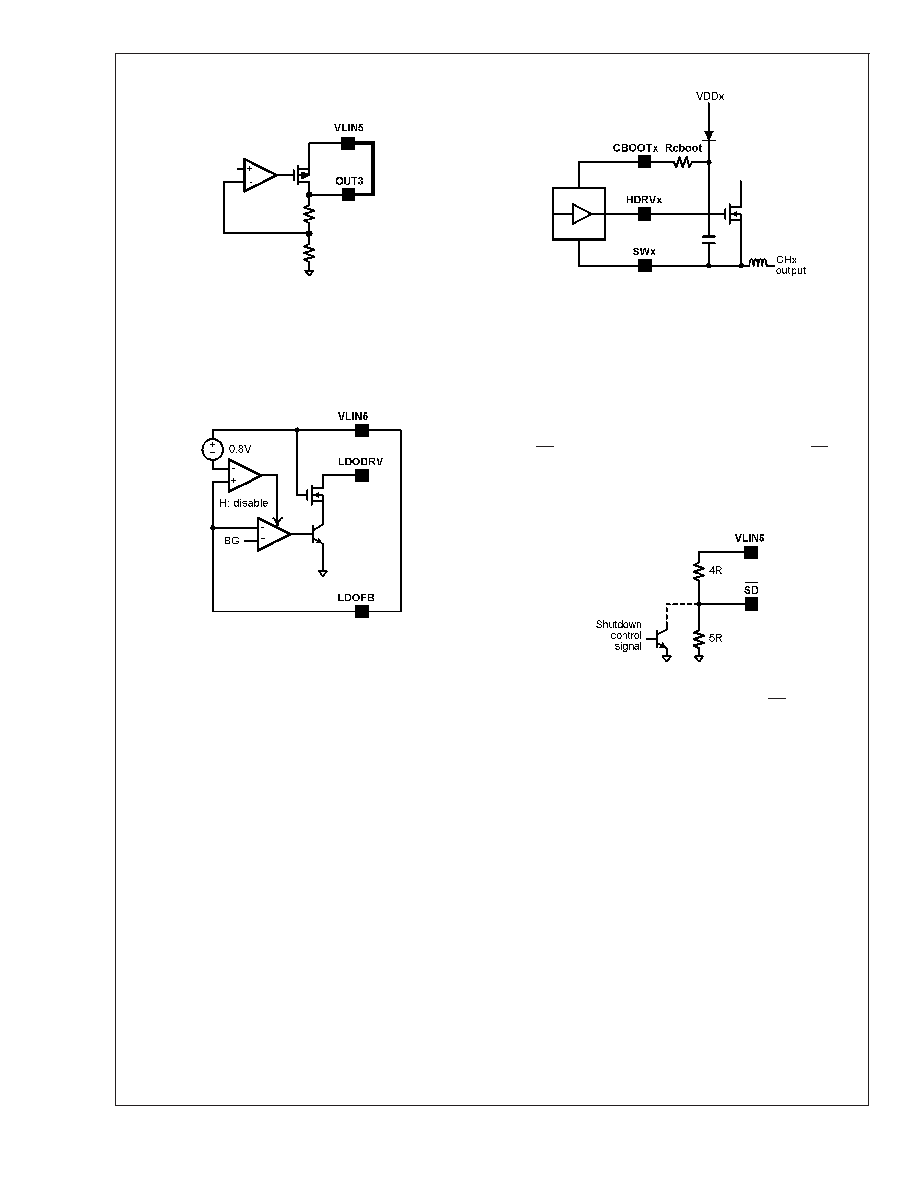
Likewise, if the LDODRV pin is not used, connect the LD-
OFB pin to VLIN5 as shown in Figure 4 to disable this
channel and the under voltage protection associated with it.
SWITCHING NOISE REDUCTION
Power MOSFETs are very fast switching devices. In syn-
chronous rectifier converter, rapid drain current rise rate of
the top FET coupled with parasitic inductance will generate
unwanted Ldi/dt spikes noise at the source node of the FET
(SWx node). The magnitude of the spike noise will increase
as the output current increases. This parasitic spike noise
may turn into electromagnetic interference (EMI) that may
cause trouble to the system performance, therefore, must be
suppressed.
As shown in Figure 5, adding a resistor in series with the
CBOOTx pin will slowdown the gate drive (HDRVx) rise time
of the top FET to yield a desired drain current transition time.
Usually a 3.3 to 5.1 ohm resistor is sufficient to suppress the
noise. The top FET switching loss will increase with higher
resistance values.
INPUT POWER SUPPLY CYCLING
If the input supply is removed during operation and then
re-applied before the power-on-reset signal has been reset,
the part will remain latched off. A solution for this problem is
shown in Figure 6, using a voltage divider of 4:5 ratio to pull
the SD pin up to VLIN5. With the voltage divider, the SD pin
always falls below the logic low level and executes the
power-on-reset after VIN drops below 3V. External shudown
control is included as an option.
DUAL-PHASE PARALLEL OUTPUTS
In applications with high output current demand, the two
switching channels can be configured to operate as a two-
phase converter to provide a single output voltage with
current sharing between the two switching channels. This
approach greatly reduces the stress and heat on the output
stage components while lowering input ripple current. Figure
7 shows a typical example for the two-phase operation.
Because precision current sense is the primary design crite-
ria to ensure accurate current sharing between the two
channels, both channels must use external sense resistors
for current sensing. To minimize the error between the error
amplifiers of the two channel, tie the feedback pins FB1_FIX
and FB2_FIX together and connect to one voltage divider for
output voltage sensing. Also, tie the COMP1 and COMP2
together and connect to the compensation network. Since
there is only one output involved, POOGD1 and 2, and VO1
and 2 should be connected in pairs for monitoring the single
output rail. ON1 and ON2 should be tied together to enable
and disable both channels simultaneously.
20015925
FIGURE 3. Connecting OUT3 to VLIN5 when not in use
20015924
FIGURE 4. Connecting LDOFB to VLIN5 to disable the
LDODRV and the UVP associated with it
20015926
FIGURE 5. Adding a resistor in series with the CBOOT
pin to suppress the turn-on switching noise
20015927
FIGURE 6. Voltage divider ratio for SD pin
LM2645
www.national.com
18
相关PDF资料 |
PDF描述 |
|---|---|
| LM2651MTCX-2.5/NOPB | 2.6 A SWITCHING REGULATOR, 345 kHz SWITCHING FREQ-MAX, PDSO16 |
| LM2651MTC-2.5/NOPB | 2.6 A SWITCHING REGULATOR, 345 kHz SWITCHING FREQ-MAX, PDSO16 |
| LM2651MTC-1.8/NOPB | 2.6 A SWITCHING REGULATOR, 345 kHz SWITCHING FREQ-MAX, PDSO16 |
| LM2670-5.0MDC | 5.4 A SWITCHING REGULATOR, 280 kHz SWITCHING FREQ-MAX, UUC |
| LM2670LDX-3.3 | 5.4 A SWITCHING REGULATOR, 280 kHz SWITCHING FREQ-MAX, PDSO14 |
相关代理商/技术参数 |
参数描述 |
|---|---|
| LM2645MTDX | 制造商:Rochester Electronics LLC 功能描述: 制造商:Texas Instruments 功能描述: |
| LM2645MTDX/NOPB | 功能描述:IC CTLR SW 2PHS 2OUTPUT 48TSSOP RoHS:是 类别:集成电路 (IC) >> PMIC - 电源管理 - 专用 系列:- 应用说明:Ultrasound Imaging Systems Application Note 产品培训模块:Lead (SnPb) Finish for COTS Obsolescence Mitigation Program 标准包装:37 系列:- 应用:医疗用超声波成像,声纳 电流 - 电源:- 电源电压:2.37 V ~ 6 V 工作温度:0°C ~ 70°C 安装类型:表面贴装 封装/外壳:56-WFQFN 裸露焊盘 供应商设备封装:56-TQFN-EP(8x8) 包装:管件 |
| LM2647 | 制造商:NSC 制造商全称:National Semiconductor 功能描述:Dual Synchronous Buck Regulator Controller |
| LM2647EVAL | 功能描述:电源管理IC开发工具 LM2647 EVAL BOARD RoHS:否 制造商:Maxim Integrated 产品:Evaluation Kits 类型:Battery Management 工具用于评估:MAX17710GB 输入电压: 输出电压:1.8 V |
| LM2647LQ | 功能描述:DC/DC 开关控制器 RoHS:否 制造商:Texas Instruments 输入电压:6 V to 100 V 开关频率: 输出电压:1.215 V to 80 V 输出电流:3.5 A 输出端数量:1 最大工作温度:+ 125 C 安装风格: 封装 / 箱体:CPAK |
发布紧急采购,3分钟左右您将得到回复。