- 您现在的位置:买卖IC网 > PDF目录358886 > LMX2312USLDX (NATIONAL SEMICONDUCTOR CORP) PLLatinum⑩ Ultra Low Power Frequency Synthesizer for RF Personal Communications PDF资料下载
参数资料
| 型号: | LMX2312USLDX |
| 厂商: | NATIONAL SEMICONDUCTOR CORP |
| 元件分类: | XO, clock |
| 英文描述: | PLLatinum⑩ Ultra Low Power Frequency Synthesizer for RF Personal Communications |
| 中文描述: | PLL FREQUENCY SYNTHESIZER, 1200 MHz, QCC20 |
| 封装: | THIN, CSP-20 |
| 文件页数: | 26/29页 |
| 文件大小: | 662K |
| 代理商: | LMX2312USLDX |
第1页第2页第3页第4页第5页第6页第7页第8页第9页第10页第11页第12页第13页第14页第15页第16页第17页第18页第19页第20页第21页第22页第23页第24页第25页当前第26页第27页第28页第29页
3.0 Programming Description
(Continued)
3.2 R REGISTER
The R register contains the R_CNTR control word and PD_POL, CPo_4X, CP_TRI, FoLD0, FoLD1 control bits. The detailed
descriptions and programming information for each control word is discussed in the following sections.
Register
Most Significant Bit
21
SHIFT REGISTER BIT LOCATION
17
16
15
14
Least Significant Bit
5
4
3
20
19
18
13
12
11
10
9
8
7
6
2
1
Address
Field
0
0
Data Field
R
FoLD1
FoLD0
CP
O
_
TRI
CP
O
_
4X
PD_
POL
R_CNTR[14:0]
0
3.2.1 R_CNTR[14:0]
The reference divider can be programmed to support divide ratios from 2 to 32,767. Divide ratios of less than 2 are prohibited.
Reference Divider (R COUNTER)
R[16:2]
Divider Value
2
3
32,767
R_CNTR[14:0]
0
0
0
0
1
1
0
0
1
0
0
1
0
0
1
0
0
1
0
0
1
0
0
1
0
0
1
0
0
1
0
0
1
0
0
1
0
0
1
1
1
1
0
1
1
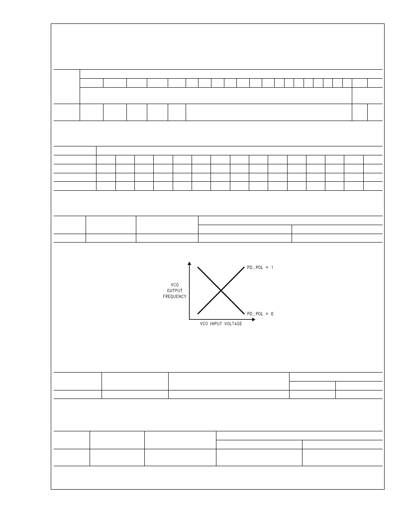
3.2.2 PD_POL
The PD_POL control bit is used to set the polarity of the phase detector based on the VCO tuning characteristic.
Phase Detector Polarity
R[17]
Control Bit Register Location
Description
Function
0
1
PD_POL
R[17]
Phase Detector Polarity Negative VCO Tuning Characteristic Positive VCO Tuning Characteristic
VCO Characteristics
20043809
3.2.3 CPo_4X
The CPo_4X control bit allows the charge pump output current magnitude to be switched from 1 mA to 4 mA. This happens
asynchronously or immediately with the change in CPo_4X bit.
Charge Pump Output Current
R[18]
Control Bit
Register Location
Description
Function
0
1
CPo_4X
R[18]
Charge Pump Output Current Magnitude
1X Current
4X Current
3.2.4 CPo_TRI
The CPo_TRI control bit allows the charge pump to be switched between a normal operating mode and a high impedance output
state. This happens asynchronously or immediately with the change in CPo_TRI bit.
Charge Pump TRI-STATE
R[19]
Control Bit
Register Location
Description
Function
0
1
CPo_TRI
R[19]
Charge Pump TRI-STATE
Charge Pump Operates Normal
Charge Pump Output in High
Impedance State
L
www.national.com
26
相关PDF资料 |
PDF描述 |
|---|---|
| LMX2312U | PLLatinum⑩ Ultra Low Power Frequency Synthesizer for RF Personal Communications |
| LMX2314 | 1.2 GHz Frequency Synthesizer for RF Personal Communications |
| LMX2314M | 1.2 GHz Frequency Synthesizer for RF Personal Communications |
| LMX2314MX | 1.2 GHz Frequency Synthesizer for RF Personal Communications |
| LMX2315 | Frequency Synthesizer for RF Personal Communications |
相关代理商/技术参数 |
参数描述 |
|---|---|
| LMX2312USLDX/NOPB | 功能描述:IC FREQ SYNTH 1.2GHZ 20LAMTCSP RoHS:是 类别:集成电路 (IC) >> 时钟/计时 - 时钟发生器,PLL,频率合成器 系列:PLLatinum™ 标准包装:39 系列:- 类型:* PLL:带旁路 输入:时钟 输出:时钟 电路数:1 比率 - 输入:输出:1:10 差分 - 输入:输出:是/是 频率 - 最大:170MHz 除法器/乘法器:无/无 电源电压:2.375 V ~ 3.465 V 工作温度:0°C ~ 70°C 安装类型:* 封装/外壳:* 供应商设备封装:* 包装:* |
| LMX2313U | 制造商:NSC 制造商全称:National Semiconductor 功能描述:PLLatinum⑩ Ultra Low Power Frequency Synthesizer for RF Personal Communications |
| LMX2313USLDX | 制造商:NSC 制造商全称:National Semiconductor 功能描述:PLLatinum⑩ Ultra Low Power Frequency Synthesizer for RF Personal Communications |
| LMX2313USLDX/NOPB | 功能描述:IC FREQ SYNTH 600MHZ 20LAMTCSP RoHS:否 类别:集成电路 (IC) >> 时钟/计时 - 时钟发生器,PLL,频率合成器 系列:PLLatinum™ 标准包装:39 系列:- 类型:* PLL:带旁路 输入:时钟 输出:时钟 电路数:1 比率 - 输入:输出:1:10 差分 - 输入:输出:是/是 频率 - 最大:170MHz 除法器/乘法器:无/无 电源电压:2.375 V ~ 3.465 V 工作温度:0°C ~ 70°C 安装类型:* 封装/外壳:* 供应商设备封装:* 包装:* |
| LMX2314 | 制造商:NSC 制造商全称:National Semiconductor 功能描述:1.2 GHz Frequency Synthesizer for RF Personal Communications |
发布紧急采购,3分钟左右您将得到回复。