参数资料
| 型号: | LNK354P |
| 厂商: | Power Integrations |
| 文件页数: | 3/16页 |
| 文件大小: | 0K |
| 描述: | IC OFFLINE SWIT OCP HV 8DIP |
| 标准包装: | 3,000 |
| 系列: | LinkSwitch®-HF |
| 输出隔离: | 隔离 |
| 频率范围: | 186kHz ~ 214kHz |
| 输出电压: | 700V |
| 功率(瓦特): | 5W |
| 工作温度: | -40°C ~ 150°C |
| 封装/外壳: | 8-DIP(0.300",7.62mm),7 引线 |
| 供应商设备封装: | DIP-8B |
| 包装: | 管件 |
�� �
�
�LNK353/354�
�V�
�LinkSwitch-HF� Functional�
�Description�
�LinkSwitch-HF� combines� a� high� voltage� power� MOSFET�
�switch� with� a� power� supply� controller� in� one� device.� Unlike�
�conventional� PWM� (pulse� width� modulator)� controllers,�
�LinkSwitch-HF� uses� a� simple� ON/OFF� control� to� regulate� the�
�output� voltage.� The� LinkSwitch-HF� controller� consists� of� an�
�oscillator,� feedback� (sense� and� logic)� circuit,� 5.8� V� regulator,�
�BYPASS� pin� under-voltage� circuit,� over-temperature� protection,�
�frequency� jittering,� current� limit� circuit,� leading� edge� blanking�
�and� a� 700� V� power� MOSFET.� The� LinkSwitch-HF� incorporates�
�additional� circuitry� for� auto-restart.�
�Oscillator�
�The� typical� oscillator� frequency� is� internally� set� to� an� average�
�of� 200� kHz.� Two� signals� are� generated� from� the� oscillator:� the�
�maximum� duty� cycle� signal� (DC� MAX� )� and� the� clock� signal� that�
�indicates� the� beginning� of� each� cycle.�
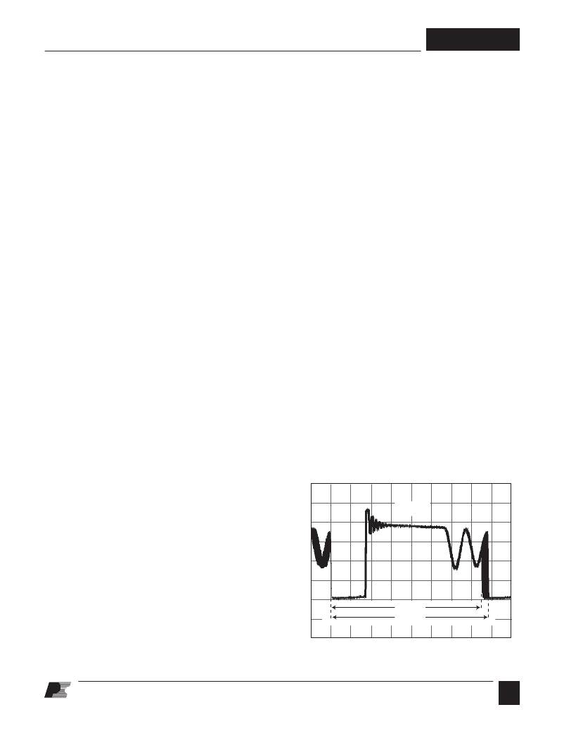
�The� LinkSwitch-HF� oscillator� incorporates� circuitry� that�
�introduces� a� small� amount� of� frequency� jitter,� typically� 16� kHz�
�peak-to-peak,� to� minimize� EMI� emission.� The� modulation� rate� of�
�the� frequency� jitter� is� set� to� 1.5� kHz� to� optimize� EMI� reduction�
�for� both� average� and� quasi-peak� emissions.� The� frequency�
�jitter� should� be� measured� with� the� oscilloscope� triggered� at�
�the� falling� edge� of� the� DRAIN� waveform.� The� waveform� in�
�Figure� 4� illustrates� the� frequency� jitter� of� the� LinkSwitch-HF� .�
�Feedback� Input� Circuit�
�The� feedback� input� circuit� at� the� FB� pin� consists� of� a� low�
�impedance� source� follower� output� set� at� 1.65� V.� When� the� current�
�delivered� into� this� pin� exceeds� 49� μ� A,� a� low� logic� level� (disable)�
�is� generated� at� the� output� of� the� feedback� circuit.� This� output�
�is� sampled� at� the� beginning� of� each� cycle� on� the� rising� edge� of�
�the� clock� signal.� If� high,� the� power� MOSFET� is� turned� on� for�
�that� cycle� (enabled),� otherwise� the� power� MOSFET� remains� off�
�(disabled).� Since� the� sampling� is� done� only� at� the� beginning� of�
�each� cycle,� subsequent� changes� in� the� FB� pin� voltage� or� current�
�during� the� remainder� of� the� cycle� are� ignored.�
�pin� through� an� external� resistor.� This� facilitates� powering� of�
�LinkSwitch-HF� externally� through� a� bias� winding� to� decrease�
�the� no-load� consumption� to� less� than� 50� mW.�
�BYPASS� Pin� Under-Voltage�
�The� BYPASS� pin� under-voltage� circuitry� disables� the� power�
�MOSFET� when� the� BYPASS� pin� voltage� drops� below� 4.85� V.�
�Once� the� BYPASS� pin� voltage� drops� below� 4.85� V,� it� must� rise�
�back� to� 5.8� V� to� enable� (turn-on)� the� power� MOSFET.�
�Over-Temperature� Protection�
�The� thermal� shutdown� circuitry� senses� the� die� temperature.�
�The� threshold� is� set� at� 142� °� C� typical� with� a� 75� °� C� hysteresis.�
�When� the� die� temperature� rises� above� this� threshold� (142� °� C)� the�
�power� MOSFET� is� disabled� and� remains� disabled� until� the� die�
�temperature� falls� by� 75� °� C,� at� which� point� it� is� re-enabled.�
�Current� Limit�
�The� current� limit� circuit� senses� the� current� in� the� power� MOSFET.�
�When� this� current� exceeds� the� internal� threshold� (I� LIMIT� ),� the�
�power� MOSFET� is� turned� off� for� the� remainder� of� that� cycle.�
�The� leading� edge� blanking� circuit� inhibits� the� current� limit�
�comparator� for� a� short� time� (t� LEB� )� after� the� power� MOSFET�
�is� turned� on.� This� leading� edge� blanking� time� has� been� set� so�
�that� current� spikes� caused� by� capacitance� and� recti?er� reverse�
�recovery� time� will� not� cause� premature� termination� of� the�
�switching� pulse.�
�Auto-Restart�
�In� the� event� of� a� fault� condition� such� as� output� overload,� output�
�short� circuit,� or� an� open� loop� condition,� LinkSwitch-HF� enters�
�into� auto-restart� operation.� An� internal� counter� clocked� by� the�
�oscillator� gets� reset� every� time� the� FB� pin� is� pulled� high.� If�
�the� FB� pin� is� not� pulled� high� for� 30� ms,� the� power� MOSFET�
�switching� is� disabled� for� 650� ms.� The� auto-restart� alternately�
�enables� and� disables� the� switching� of� the� power� MOSFET� until�
�the� fault� condition� is� removed.�
�600�
�500�
�DRAIN�
�5.8� V� Regulator� and� 6.3� V� Shunt� Voltage� Clamp�
�The� 5.8� V� regulator� charges� the� bypass� capacitor� connected�
�to� the� BYPASS� pin� to� 5.8� V� by� drawing� a� current� from� the�
�voltage� on� the� DRAIN,� whenever� the� MOSFET� is� off.� The�
�BYPASS� pin� is� the� internal� supply� voltage� node� for� the�
�LinkSwitch-HF� .� When� the� MOSFET� is� on,� the� LinkSwitch-HF�
�runs� off� of� the� energy� stored� in� the� bypass� capacitor.� Extremely�
�low� power� consumption� of� the� internal� circuitry� allows� the�
�LinkSwitch-HF� to� operate� continuously� from� the� current� drawn�
�from� the� DRAIN� pin.� A� bypass� capacitor� value� of� 0.1� μ� F� is� suf?cient�
�for� both� high� frequency� decoupling� and� energy� storage.�
�400�
�300�
�200�
�100�
�0�
�208� kHz�
�192� kHz�
�In� addition,� there� is� a� 6.3� V� shunt� regulator� clamping� the�
�BYPASS� pin� at� 6.3� V� when� current� is� provided� to� the� BYPASS�
�0�
�Figure� 4.� Frequency� Jitter.�
�Time� (� μ� s)�
�F�
�2/05�
�6.4�
�3�
�相关PDF资料 |
PDF描述 |
|---|---|
| LNK501P | IC SWIT OCP CV/CC HV 8DIP |
| LNK584GG | IC OFFLINE SWITCHER 3W 8-SMD |
| LOC110S | OPTOCOUPLER TRANSISTOR 8-SMD |
| LOC111S | OPTOCOUPLER TRANSISTOR 8-SMD |
| LOC112S | OPTOCOUPLER TRANSISTOR 8-SMD |
相关代理商/技术参数 |
参数描述 |
|---|---|
| LNK354PN | 功能描述:交流/直流开关转换器 4.5W (85-265 VAC) 5W (230 VAC) RoHS:否 制造商:STMicroelectronics 输出电压:800 V 输入/电源电压(最大值):23.5 V 输入/电源电压(最小值):11.5 V 开关频率:115 kHz 电源电流:1.6 mA 工作温度范围:- 40 C to + 150 C 安装风格:SMD/SMT 封装 / 箱体:SSO-10 封装:Reel |
| LNK3604D-TL | 功能描述:IC OFFLN CONV FLYBACK 8SO 制造商:power integrations 系列:LinkSwitch?-XT2 包装:剪切带(CT) 零件状态:在售 输出隔离:隔离 内部开关:是 电压 - 击穿:725V 拓扑:反激 电压 - 电源(Vcc/Vdd):- 占空比:69% 频率 - 开关:132kHz 功率(W):7.3W 故障保护:限流,超温,过压 控制特性:- 工作温度:-40°C ~ 150°C(TJ) 封装/外壳:8-SOIC(0.154",3.90mm 宽),7 引线 供应商器件封装:8-SO 安装类型:表面贴装 标准包装:1 |
| LNK3604G-TL | 功能描述:IC OFFLN CONV FLYBACK 8SMD 制造商:power integrations 系列:LinkSwitch?-XT2 包装:剪切带(CT) 零件状态:在售 输出隔离:隔离 内部开关:是 电压 - 击穿:725V 拓扑:反激 电压 - 电源(Vcc/Vdd):- 占空比:69% 频率 - 开关:132kHz 功率(W):7.3W 故障保护:限流,超温,过压 控制特性:- 工作温度:-40°C ~ 150°C(TJ) 封装/外壳:8-SMD(7 个接脚),鸥形翼 供应商器件封装:8-SMD 安装类型:表面贴装 标准包装:1 |
| LNK3604P | 功能描述:IC OFFLN CONV FLYBACK 8DIP 制造商:power integrations 系列:LinkSwitch?-XT2 包装:管件 零件状态:在售 输出隔离:隔离 内部开关:是 电压 - 击穿:725V 拓扑:反激 电压 - 电源(Vcc/Vdd):- 占空比:69% 频率 - 开关:132kHz 功率(W):7.3W 故障保护:限流,超温,过压 控制特性:- 工作温度:-40°C ~ 150°C(TJ) 封装/外壳:8-DIP(0.300",7.62mm),7 引线 供应商器件封装:DIP-8C 安装类型:通孔 标准包装:50 |
| LNK362 | 制造商:POWERINT 制造商全称:Power Integrations, Inc. 功能描述:Energy Effi cient, Low Power Off-Line Switcher IC |
发布紧急采购,3分钟左右您将得到回复。