参数资料
| 型号: | LNK354P |
| 厂商: | Power Integrations |
| 文件页数: | 6/16页 |
| 文件大小: | 0K |
| 描述: | IC OFFLINE SWIT OCP HV 8DIP |
| 标准包装: | 3,000 |
| 系列: | LinkSwitch®-HF |
| 输出隔离: | 隔离 |
| 频率范围: | 186kHz ~ 214kHz |
| 输出电压: | 700V |
| 功率(瓦特): | 5W |
| 工作温度: | -40°C ~ 150°C |
| 封装/外壳: | 8-DIP(0.300",7.62mm),7 引线 |
| 供应商设备封装: | DIP-8B |
| 包装: | 管件 |
�� �
�
�LNK353/354�
�of� the� diode� for� heatsinking.� A� larger� area� is� preferred� at� the�
�quiet� cathode� terminal.� A� large� anode� area� can� increase� high�
�frequency� radiated� EMI.�
�Quick� Design� Checklist�
�As� with� any� power� supply� design,� all� LinkSwitch-HF� designs�
�should� be� veri?ed� on� the� bench� to� make� sure� that� component�
�speci?cations� are� not� exceeded� under� worst-case� conditions.� The�
�following� minimum� set� of� tests� is� strongly� recommended:�
�1.� Maximum� drain� voltage� –� Verify� that� V� DS� does� not� exceed�
�675� V� at� the� highest� input� voltage� and� peak� (overload)� output�
�power.�
�2.� Maximum� drain� current� –� At� maximum� ambient� temperature,�
�maximum� input� voltage� and� peak� output� (overload)� power,�
�verify� drain� current� waveforms� for� any� signs� of� transformer�
�saturation� and� excessive� leading� edge� current� spikes� at�
�startup.� Repeat� under� steady� state� conditions� and� verify� that�
�the� leading� edge� current� spike� event� is� below� I� LIMIT(MIN)� at� the�
�end� of� the� t� LEB(MIN)� .� Under� all� conditions,� the� maximum� drain�
�current� should� be� below� the� speci?ed� absolute� maximum�
�ratings.�
�3.� Thermal� Check� –� At� speci?ed� maximum� output� power,�
�minimum� input� voltage� and� maximum� ambient� temperature,�
�verify� that� the� temperature� speci?cations� are� not� exceeded�
�for� LinkSwitch-HF� ,� transformer,� output� diode,� and� output�
�capacitors.� Enough� thermal� margin� should� be� allowed� for�
�part-to-part� variation� of� the� R� DS(ON)� of� LinkSwitch-HF� as�
�speci?ed� in� the� data� sheet.� Under� low� line,� maximum� power,�
�a� maximum� LinkSwitch-HF� SOURCE� pin� temperature� of�
�100� °C� is� recommended� to� allow� for� these� variations.�
�Design� Tools�
�Up-to-date� information� on� design� tools� can� be� found� at� the�
�Power� Integrations� website:� www.powerint.com.�
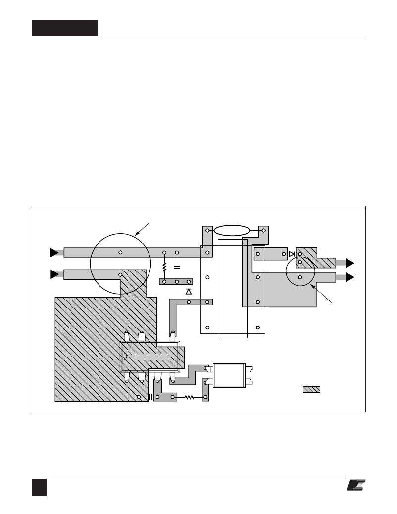
�+�
�TOP� VIEW�
�INPUT� FILTER�
�CAPACITOR�
�Y1-�
�CAPACITOR�
�HV� DC�
�INPUT�
�-�
�T�
�R�
�A�
�N�
�S�
�F�
�O�
�R�
�+�
�DC�
�OUT�
�-�
�S�
�S�
�D�
�PRI�
�M�
�E�
�R�
�SEC�
�OUTPUT� FILTER�
�CAPACITOR�
�LinkSwitch-HF�
�S�
�S�
�BP�
�FB�
�OPTO-�
�COUPLER�
�MAXIMIZE� HATCHED� COPPER�
�AREAS� (� )� FOR� OPTIMUM�
�HEATSINKING�
�C� BP�
�Figure� 6.� Recommended� Printed� Circuit� Layout� for� LinkSwitch-HF� in� a� Flyback� Converter� Con?guration.�
�PI-3890-102704�
�6�
�F�
�2/05�
�相关PDF资料 |
PDF描述 |
|---|---|
| LNK501P | IC SWIT OCP CV/CC HV 8DIP |
| LNK584GG | IC OFFLINE SWITCHER 3W 8-SMD |
| LOC110S | OPTOCOUPLER TRANSISTOR 8-SMD |
| LOC111S | OPTOCOUPLER TRANSISTOR 8-SMD |
| LOC112S | OPTOCOUPLER TRANSISTOR 8-SMD |
相关代理商/技术参数 |
参数描述 |
|---|---|
| LNK354PN | 功能描述:交流/直流开关转换器 4.5W (85-265 VAC) 5W (230 VAC) RoHS:否 制造商:STMicroelectronics 输出电压:800 V 输入/电源电压(最大值):23.5 V 输入/电源电压(最小值):11.5 V 开关频率:115 kHz 电源电流:1.6 mA 工作温度范围:- 40 C to + 150 C 安装风格:SMD/SMT 封装 / 箱体:SSO-10 封装:Reel |
| LNK3604D-TL | 功能描述:IC OFFLN CONV FLYBACK 8SO 制造商:power integrations 系列:LinkSwitch?-XT2 包装:剪切带(CT) 零件状态:在售 输出隔离:隔离 内部开关:是 电压 - 击穿:725V 拓扑:反激 电压 - 电源(Vcc/Vdd):- 占空比:69% 频率 - 开关:132kHz 功率(W):7.3W 故障保护:限流,超温,过压 控制特性:- 工作温度:-40°C ~ 150°C(TJ) 封装/外壳:8-SOIC(0.154",3.90mm 宽),7 引线 供应商器件封装:8-SO 安装类型:表面贴装 标准包装:1 |
| LNK3604G-TL | 功能描述:IC OFFLN CONV FLYBACK 8SMD 制造商:power integrations 系列:LinkSwitch?-XT2 包装:剪切带(CT) 零件状态:在售 输出隔离:隔离 内部开关:是 电压 - 击穿:725V 拓扑:反激 电压 - 电源(Vcc/Vdd):- 占空比:69% 频率 - 开关:132kHz 功率(W):7.3W 故障保护:限流,超温,过压 控制特性:- 工作温度:-40°C ~ 150°C(TJ) 封装/外壳:8-SMD(7 个接脚),鸥形翼 供应商器件封装:8-SMD 安装类型:表面贴装 标准包装:1 |
| LNK3604P | 功能描述:IC OFFLN CONV FLYBACK 8DIP 制造商:power integrations 系列:LinkSwitch?-XT2 包装:管件 零件状态:在售 输出隔离:隔离 内部开关:是 电压 - 击穿:725V 拓扑:反激 电压 - 电源(Vcc/Vdd):- 占空比:69% 频率 - 开关:132kHz 功率(W):7.3W 故障保护:限流,超温,过压 控制特性:- 工作温度:-40°C ~ 150°C(TJ) 封装/外壳:8-DIP(0.300",7.62mm),7 引线 供应商器件封装:DIP-8C 安装类型:通孔 标准包装:50 |
| LNK362 | 制造商:POWERINT 制造商全称:Power Integrations, Inc. 功能描述:Energy Effi cient, Low Power Off-Line Switcher IC |
发布紧急采购,3分钟左右您将得到回复。