参数资料
| 型号: | LNK501P |
| 厂商: | Power Integrations |
| 文件页数: | 5/20页 |
| 文件大小: | 0K |
| 描述: | IC SWIT OCP CV/CC HV 8DIP |
| 标准包装: | 3,000 |
| 系列: | LinkSwitch® |
| 输出隔离: | 隔离 |
| 频率范围: | 26kHz ~ 46kHz |
| 输出电压: | 700V |
| 功率(瓦特): | 4W |
| 工作温度: | -40°C ~ 150°C |
| 封装/外壳: | 8-DIP(0.300",7.62mm),7 引线 |
| 供应商设备封装: | DIP-8B |
| 包装: | 管件 |
| 配用: | 596-1001-ND - KIT DESIGN ACCELERATOR ADAPTER |
�� �
�
�LNK501�
�instead� placed� on� the� cathode� side� of� D1,� it� would� become� a�
�switching� node,� generating� additional� common� mode� EMI�
�currents� through� its� internal� parasitic� capacitance.�
�The� feedback� con?guration� in� Figure� 6� is� simply� a� resistive�
�divider� made� up� of� R1� and� R3� with� D1,� R2,� C1� and� C2� rectifying,�
�?ltering� and� smoothing� the� primary� winding� voltage� signal.� The�
�optocoupler� therefore� effectively� adjusts� the� resistor� divider� ratio�
�to� control� the� DC� voltage� across� R1� and� therefore,� the� feedback�
�current� received� by� the� LinkSwitch� CONTROL� pin.�
�When� the� power� supply� operates� in� the� constant� current� (CC)�
�region,� for� example� when� charging� a� battery,� the� output� voltage�
�is� below� the� voltage� feedback� threshold� de?ned� by� U1� and�
�VR1� and� the� optocoupler� is� fully� off.� In� this� region,� the� circuit�
�behaves� exactly� as� previously� described� with� reference� to�
�Figure� 5� where� the� re?ected� voltage� increases� with� increasing�
�output� voltage� and� the� LinkSwitch� internal� current� limit� is�
�adjusted� to� provide� an� approximate� CC� output� characteristic.�
�Note� that� for� similar� output� characteristics� in� the� CC� region,�
�the� value� of� R1� in� Figure� 5� will� be� equal� to� the� value� of� R1+R3�
�in� Figure� 6.�
�When� the� output� reaches� the� voltage� feedback� threshold� set� by�
�U1� and� VR1,� the� optocoupler� turns� on.� Any� further� increase�
�in� the� power� supply� output� voltage� results� in� the� U1� transistor�
�current� increasing,� which� increases� the� percentage� of� the�
�re?ected� voltage� appearing� across� R1.� The� resulting� increase�
�in� the� LinkSwitch� CONTROL� current� reduces� the� duty� cycle�
�according� to� Figure� 4� and� therefore,� maintains� the� output�
�voltage� regulation.�
�Normally,� R1� and� R3� are� chosen� to� be� equal� in� value.� However,�
�increasing� R3� (while� reducing� R1� to� keep� R1� +� R3� constant)�
�increases� loop� gain� in� the� CV� region,� improving� load� regulation.�
�The� extent� to� which� R3� can� be� increased� is� limited� by� opto�
�transistor� voltage� and� dissipation� ratings� and� should� be� fully�
�tested� before� ?nalizing� a� design.� The� values� of� C2� and� C3� are�
�less� important� other� than� to� make� sure� they� are� large� enough�
�to� have� very� little� in?uence� on� the� impedance� of� the� voltage�
�division� circuit� set� up� by� R1,� R3� and� U1� at� the� switching�
�frequency.� Normally,� the� values� of� C2� and� C3� in� Figure� 6� are�
�chosen� equal� to� the� value� of� C2� in� Figure� 5,� though� the� voltage�
�rating� may� be� reduced� depending� on� the� relative� values� of� R1�
�and� R2� discussed� above.� See� Applications� section� for� typical�
�values� of� components.�
�Figure� 7� shows� the� in?uence� of� optocoupler� feedback� on� the�
�output� characteristic.� The� envelope� de?ned� by� the� dashed� lines�
�represent� the� worst� case� power� supply� DC� output� voltage� and�
�current� tolerances� (unit-to-unit� and� over� the� input� voltage�
�range)� if� an� optocoupler� is� not� used.� A� typical� example� of� an�
�inherent� (without� optocoupler)� output� characteristic� is� shown�
�dotted.� This� is� the� characteristic� that� would� result� if� U1,� R4� and�
�VR1� were� removed.� The� optocoupler� feedback� results� in� the�
�characteristic� shown� by� the� solid� line.� The� load� variation� arrow� in�
�Figure� 7� represents� the� locus� of� the� output� characteristic� normally�
�seen� during� a� battery� charging� cycle.� The� two� characteristics�
�are� identical� as� the� output� voltage� rises� but� then� separate� as�
�shown� when� the� voltage� feedback� threshold� is� reached.� This�
�is� the� characteristic� seen� if� the� voltage� feedback� threshold� is�
�above� the� output� voltage� at� the� inherent� CC� to� CV� transition�
�point� also� indicated� in� Figure� 7.�
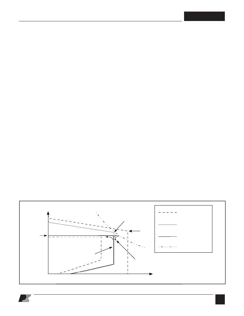
�Figure� 8� shows� a� case� where� the� voltage� feedback� threshold� is�
�set� below� the� voltage� at� the� inherent� CC� to� CV� transition� point.�
�In� this� case,� as� the� output� voltage� rises,� the� secondary� feedback�
�circuit� takes� control� before� the� inherent� CC� to� CV� transition�
�occurs.� In� an� actual� battery� charging� application,� this� simply�
�limits� the� output� voltage� to� a� lower� value.�
�OUTPUT� VOLTAGE�
�VOLTAGE�
�FEEDBACK�
�THRESHOLD�
�INHERENT�
�CC� TO� CV�
�TRANSITION�
�POINT�
�V� O(MAX)�
�TOLERANCE� ENVELOPE�
�WITHOUT� OPTOCOUPLER�
�TYPICAL� INHERENT�
�CHARACTERISTIC� WITHOUT�
�OPTOCOUPLER�
�CHARACTERISTIC� WITH�
�OPTOCOUPLER�
�POWER� SUPPLY� PEAK�
�LOAD� VARIATION�
�DURING� BATTERY�
�CHARGING�
�OUTPUT� POWER� CURVE�
�CHARACTERISTIC� OBSERVED� WITH�
�LOAD� VARIATION� OFTEN� APPLIED� DURING�
�LABORATORY� BENCH� TESTING�
�OUTPUT� CURRENT�
�Figure� 8.� Output� Characteristic� with� Optocoupler� Regulation� (Reduced� Voltage� Feedback� Threshold).�
�PI-2790-112102�
�I�
�2/05�
�5�
�相关PDF资料 |
PDF描述 |
|---|---|
| LNK584GG | IC OFFLINE SWITCHER 3W 8-SMD |
| LOC110S | OPTOCOUPLER TRANSISTOR 8-SMD |
| LOC111S | OPTOCOUPLER TRANSISTOR 8-SMD |
| LOC112S | OPTOCOUPLER TRANSISTOR 8-SMD |
| LP2950ACDT-3.3RG | IC REG LDO 3.3V .1A DPAK |
相关代理商/技术参数 |
参数描述 |
|---|---|
| LNK501P_1 | 制造商:POWERINT 制造商全称:Power Integrations, Inc. 功能描述:2.2W Cell Phone Charger |
| LNK501PN | 功能描述:交流/直流开关转换器 3W 85-265 VAC 4W 230 VAC RoHS:否 制造商:STMicroelectronics 输出电压:800 V 输入/电源电压(最大值):23.5 V 输入/电源电压(最小值):11.5 V 开关频率:115 kHz 电源电流:1.6 mA 工作温度范围:- 40 C to + 150 C 安装风格:SMD/SMT 封装 / 箱体:SSO-10 封装:Reel |
| LNK520 | 制造商:POWERINT 制造商全称:Power Integrations, Inc. 功能描述:Energy Efficient, CV or CV/CC Switcher for Very Low Cost Adapters and Chargers |
| LNK520G | 功能描述:IC SWIT OCP CV/CC HV 8SMD RoHS:否 类别:集成电路 (IC) >> PMIC - AC-DC 转换器,离线开关 系列:LinkSwitch® 标准包装:1 系列:FPS™ 输出隔离:隔离 频率范围:61kHz ~ 73kHz 输入电压:8 V ~ 26 V 输出电压:650V 功率(瓦特):12W 工作温度:-40°C ~ 115°C 封装/外壳:8-DIP(0.300",7.62mm) 供应商设备封装:8-MDIP 包装:Digi-Reel® 其它名称:FSL206MRBNFSDKR |
| LNK520GN | 功能描述:交流/直流开关转换器 3W 85-265 VAC 4W 230 VAC RoHS:否 制造商:STMicroelectronics 输出电压:800 V 输入/电源电压(最大值):23.5 V 输入/电源电压(最小值):11.5 V 开关频率:115 kHz 电源电流:1.6 mA 工作温度范围:- 40 C to + 150 C 安装风格:SMD/SMT 封装 / 箱体:SSO-10 封装:Reel |
发布紧急采购,3分钟左右您将得到回复。