- 您现在的位置:买卖IC网 > PDF目录14798 > LT1054IS8#PBF (Linear Technology)IC REG SWITCHD CAP DBL INV 8SOIC PDF资料下载
参数资料
| 型号: | LT1054IS8#PBF |
| 厂商: | Linear Technology |
| 文件页数: | 7/16页 |
| 文件大小: | 0K |
| 描述: | IC REG SWITCHD CAP DBL INV 8SOIC |
| 标准包装: | 100 |
| 类型: | 切换式电容器(充电泵),倍增器,反相 |
| 输出类型: | 可调式 |
| 输出数: | 1 |
| 输出电压: | 可调 |
| 输入电压: | 3.5 V ~ 15 V |
| 频率 - 开关: | 25kHz |
| 电流 - 输出: | 100mA |
| 同步整流器: | 无 |
| 工作温度: | -40°C ~ 100°C |
| 安装类型: | 表面贴装 |
| 封装/外壳: | 8-SOIC(0.154",3.90mm 宽) |
| 包装: | 管件 |
| 供应商设备封装: | 8-SOIC |
| 产品目录页面: | 1339 (CN2011-ZH PDF) |
�� ��
��
��LT1054/LT1054L�
�PIN� FUNCTIONS�
�is� charging,� the� peak� supply� current� will� be� approximately�
�equal� to� 2.2� times� the� output� current.� During� the� time� that�
�C� IN� is� delivering� charge� to� C� OUT� the� supply� current� drops�
�to� approximately� 0.2� times� the� output� current.� An� input�
�supply� bypass� capacitor� will� supply� part� of� the� peak� input�
�current� drawn� by� the� LT1054� and� average� out� the� current�
�drawn� from� the� supply.� A� minimum� input� supply� bypass�
�APPLICATIONS� INFORMATION�
�capacitor� of� 2μF,� preferably� tantalum� or� some� other� low� ESR�
�type� is� recommended.� A� larger� capacitor� may� be� desirable�
�in� some� cases,� for� example,� when� the� actual� input� supply�
�is� connected� to� the� LT1054� through� long� leads,� or� when�
�the� pulse� current� drawn� by� the� LT1054� might� affect� other�
�circuitry� through� supply� coupling.�
�Theory� of� Operation�
�To� understand� the� theory� of� operation� of� the� LT1054,� a� re-�
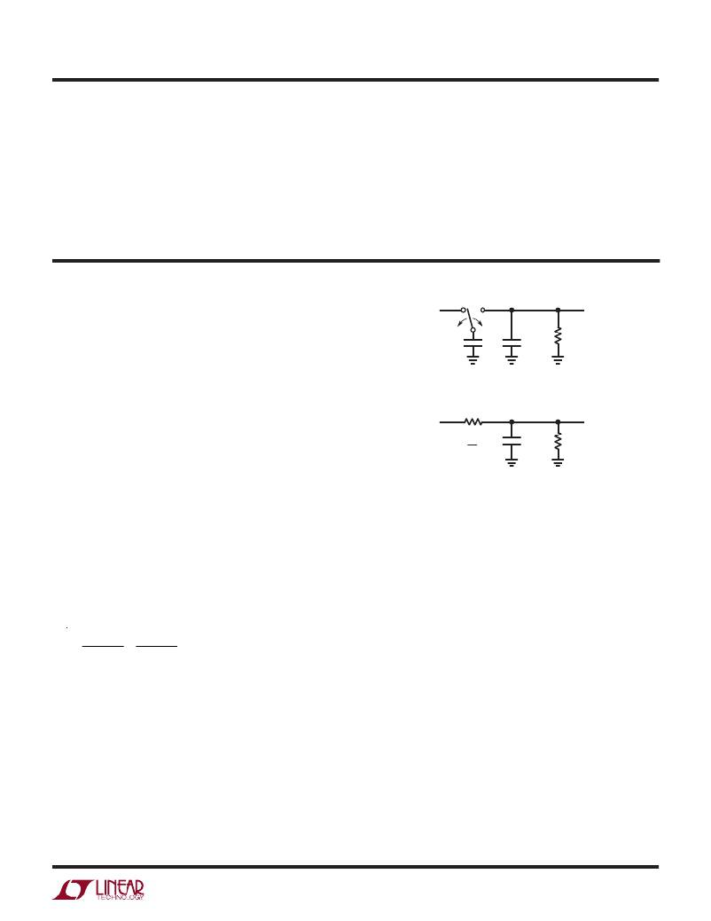
�view� of� a� basic� switched-capacitor� building� block� is� helpful.�
�V1�
�f�
�C1�
�C2�
�R� L�
�V2�
�R� EQUIV� =� 1�
�I� =�
�=�
�InFigure3whentheswitchisintheleftposition,capaci-�
�tor� C1� will� charge� to� voltage� V1.� The� total� charge� on� C1�
�will� be� q1� =� C1V1.� The� switch� then� moves� to� the� right,�
�discharging� C1� to� voltage� V2.� After� this� discharge� time�
�the� charge� on� C1� is� q2� =� C1V2.� Note� that� charge� has� been�
�transferred� from� the� source� V1� to� the� output� V2.� The�
�amount� of� charge� transferred� is:�
�?� q� =� q1� –� q2� =� C1(V1� –� V2)�
�If� the� switch� is� cycled� f� times� per� second,� the� charge�
�transfer� per� unit� time� (i.e.,� current)� is:�
�I� =� (f)(� ?� q)� =� (f)[C1(V1� –� V2)]�
�To� obtain� an� equivalent� resistance� for� the� switched-�
�capacitor� network� we� can� rewrite� this� equation� in� terms�
�of� voltage� and� impedance� equivalence:�
�V1– V2 V1– V2�
�1/� fC1� R� EQUIV�
�A� new� variable� R� EQUIV� is� defined� such� that� R� EQUIV� =� 1/fC1.�
�Thus� the� equivalent� circuit� for� the� switched-capacitor�
�network� is� as� shown� in� Figure� 4.� The� LT1054� has� the� same�
�switching� action� as� the� basic� switched-capacitor� building�
�block.� Even� though� this� simplification� doesn’t� include� finite�
�switch� on-resistance� and� output� voltage� ripple,� it� provides�
�an� intuitive� feel� for� how� the� device� works.�
�These� simplified� circuits� explain� voltage� loss� as� a� function�
�of� frequency� (see� Typical� Performance� Characteristics).�
�As� frequency� is� decreased,� the� output� impedance� will�
�LT1054� ?� F03�
�Figure� 3.� Switched-Capacitor� Building� Block�
�R� EQUIV�
�V1� V2�
�C2� R� L�
�fC1�
�LT1054� ?� F04�
�Figure� 3.� Switched-Capacitor� Equivalent� Circuit�
�eventually� be� dominated� by� the� 1/fC1� term� and� voltage�
�losses� will� rise.�
�Note� that� losses� also� rise� as� frequency� increases.� This� is�
�caused� by� internal� switching� losses� which� occur� due� to�
�some� finite� charge� being� lost� on� each� switching� cycle.� This�
�charge� loss� per-unit-cycle,� when� multiplied� by� the� switching�
�frequency,� becomes� a� current� loss.� At� high� frequency� this�
�loss� becomes� significant� and� voltage� losses� again� rise.�
�The� oscillator� of� the� LT1054� is� designed� to� run� in� the�
�frequency� band� where� voltage� losses� are� at� a� minimum.�
�Regulation�
�The� error� amplifier� of� the� LT1054� servos� the� drive� to� the�
�PNP� switch� to� control� the� voltage� across� the� input� capaci-�
�tor� (C� IN� )� which� in� turn� will� determine� the� output� voltage.�
�Using� the� reference� and� error� amplifier� of� the� LT1054,�
�an� external� resistive� divider� is� all� that� is� needed� to� set�
�the� regulated� output� voltage.� Figure� 5� shows� the� basic�
�regulator� configuration� and� the� formula� for� calculating�
�the� appropriate� resistor� values.� R1� should� be� chosen� to�
�1954lfg�
�7�
�相关PDF资料 |
PDF描述 |
|---|---|
| LT1766IGN#PBF | IC REG BUCK ADJ 1.5A 16SSOP |
| ESC20DREN-S13 | CONN EDGECARD 40POS .100 EXTEND |
| LT3508HFE#PBF | IC REG BUCK ADJ 1.4A DL 16TSSOP |
| LT1071CT#PBF | IC REG MULTI CONFIG ADJ TO220-5 |
| LT1171CT#PBF | IC REG MULTI CONFIG ADJ TO220-5 |
相关代理商/技术参数 |
参数描述 |
|---|---|
| LT1054ISW | 功能描述:IC REG MULTI CONFIG ADJ 16SOIC RoHS:否 类别:集成电路 (IC) >> PMIC - 稳压器 - DC DC 开关稳压器 系列:- 设计资源:Design Support Tool 标准包装:1 系列:- 类型:升压(升压) 输出类型:固定 输出数:1 输出电压:3V 输入电压:0.75 V ~ 2 V PWM 型:- 频率 - 开关:- 电流 - 输出:100mA 同步整流器:是 工作温度:-40°C ~ 85°C 安装类型:表面贴装 封装/外壳:SOT-23-5 细型,TSOT-23-5 包装:剪切带 (CT) 供应商设备封装:TSOT-23-5 其它名称:AS1323-BTTT-30CT |
| LT1054ISW#PBF | 功能描述:IC REG MULTI CONFIG ADJ 16SOIC RoHS:是 类别:集成电路 (IC) >> PMIC - 稳压器 - DC DC 开关稳压器 系列:- 产品培训模块:MIC23xxx HyperLight Load™ Regulators 标准包装:5,000 系列:HyperLight Load® 类型:降压(降压) 输出类型:固定 输出数:1 输出电压:1.8V 输入电压:2.7 V ~ 5.5 V PWM 型:混合物 频率 - 开关:4MHz 电流 - 输出:2A 同步整流器:是 工作温度:-40°C ~ 125°C 安装类型:表面贴装 封装/外壳:8-VFDFN 裸露焊盘,8-MLF? 包装:带卷 (TR) 供应商设备封装:8-MLF?(2x2) 产品目录页面:1094 (CN2011-ZH PDF) 其它名称:576-3303-2 |
| LT1054ISW#TR | 功能描述:IC REG MULTI CONFIG ADJ 16SOIC RoHS:否 类别:集成电路 (IC) >> PMIC - 稳压器 - DC DC 开关稳压器 系列:- 设计资源:Design Support Tool 标准包装:1 系列:- 类型:升压(升压) 输出类型:固定 输出数:1 输出电压:3V 输入电压:0.75 V ~ 2 V PWM 型:- 频率 - 开关:- 电流 - 输出:100mA 同步整流器:是 工作温度:-40°C ~ 85°C 安装类型:表面贴装 封装/外壳:SOT-23-5 细型,TSOT-23-5 包装:剪切带 (CT) 供应商设备封装:TSOT-23-5 其它名称:AS1323-BTTT-30CT |
| LT1054ISW#TRPBF | 功能描述:IC REG MULTI CONFIG ADJ 16SOIC RoHS:是 类别:集成电路 (IC) >> PMIC - 稳压器 - DC DC 开关稳压器 系列:- 设计资源:Design Support Tool 标准包装:1 系列:- 类型:升压(升压) 输出类型:固定 输出数:1 输出电压:3V 输入电压:0.75 V ~ 2 V PWM 型:- 频率 - 开关:- 电流 - 输出:100mA 同步整流器:是 工作温度:-40°C ~ 85°C 安装类型:表面贴装 封装/外壳:SOT-23-5 细型,TSOT-23-5 包装:剪切带 (CT) 供应商设备封装:TSOT-23-5 其它名称:AS1323-BTTT-30CT |
| LT1054LCS8 | 功能描述:IC REG MULTI CONFIG ADJ 8SOIC RoHS:否 类别:集成电路 (IC) >> PMIC - 稳压器 - DC DC 开关稳压器 系列:- 标准包装:2,500 系列:- 类型:升压(升压) 输出类型:可调式 输出数:1 输出电压:1.24 V ~ 30 V 输入电压:1.5 V ~ 12 V PWM 型:电流模式,混合 频率 - 开关:600kHz 电流 - 输出:500mA 同步整流器:无 工作温度:-40°C ~ 85°C 安装类型:表面贴装 封装/外壳:8-SOIC(0.154",3.90mm 宽) 包装:带卷 (TR) 供应商设备封装:8-SOIC |
发布紧急采购,3分钟左右您将得到回复。