- 您现在的位置:买卖IC网 > PDF目录14798 > LT1054IS8#PBF (Linear Technology)IC REG SWITCHD CAP DBL INV 8SOIC PDF资料下载
参数资料
| 型号: | LT1054IS8#PBF |
| 厂商: | Linear Technology |
| 文件页数: | 9/16页 |
| 文件大小: | 0K |
| 描述: | IC REG SWITCHD CAP DBL INV 8SOIC |
| 标准包装: | 100 |
| 类型: | 切换式电容器(充电泵),倍增器,反相 |
| 输出类型: | 可调式 |
| 输出数: | 1 |
| 输出电压: | 可调 |
| 输入电压: | 3.5 V ~ 15 V |
| 频率 - 开关: | 25kHz |
| 电流 - 输出: | 100mA |
| 同步整流器: | 无 |
| 工作温度: | -40°C ~ 100°C |
| 安装类型: | 表面贴装 |
| 封装/外壳: | 8-SOIC(0.154",3.90mm 宽) |
| 包装: | 管件 |
| 供应商设备封装: | 8-SOIC |
| 产品目录页面: | 1339 (CN2011-ZH PDF) |
�� �
�
�LT1054/LT1054L�
�APPLICATIONS� INFORMATION�
�+�
�C� IN�
�wheredV=peak-to-peakrippleandf=oscillatorfrequency.�
�For� output� capacitors� with� significant� ESR� a� second� term�
�must� be� added� to� account� for� the� voltage� step� at� the� switch�
�transitions.� This� step� is� approximately� equal� to:�
�(2I� OUT� )(ESR� of� C� OUT� )�
�Power� Dissipation�
�The� power� dissipation� of� any� LT1054� circuit� must� be�
�limited� such� that� the� junction� temperature� of� the� device�
�does� not� exceed� the� maximum� junction� temperature� rat-�
�ings.� The� total� power� dissipation� must� be� calculated� from�
�two� components,� the� power� loss� due� to� voltage� drops�
�in� the� switches� and� the� power� loss� due� to� drive� current�
�losses.� The� total� power� dissipated� by� the� LT1054� can� be�
�calculated� from:�
�P� ≈� (V� IN� –� |� V� OUT� |� )(I� OUT� )� +� (V� IN� )(I� OUT� )(0.2)�
�where� both� V� IN� and� V� OUT� are� referred� to� the� ground� pin�
�(Pin?3)� of� the� LT1054.� For� LT1054� regulator� circuits,� the�
�power� dissipation� will� be� equivalent� to� that� of� a� linear�
�regulator.� Due� to� the� limited� power� handling� capability� of�
�the� LT1054� packages,� the� user� will� have� to� limit� output�
�current� requirements� or� take� steps� to� dissipate� some� power�
�external� to� the� LT1054� for� large� input/output� differentials.�
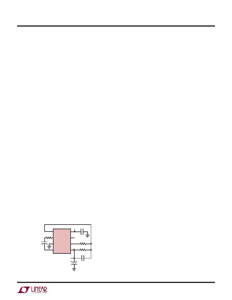
�This� can� be� accomplished� by� placing� a� resistor� in� series�
�with� C� IN� as� shown� in� Figure� 6.� A� portion� of� the� input�
�voltage� will� then� be� dropped� across� this� resistor� without�
�affecting� the� output� regulation.� Because� switch� current� is�
�approximately� 2.2� times� the� output� current� and� the� resistor�
�will� cause� a� voltage� drop� when� C� IN� is� both� charging� and�
�discharging,� the� resistor� should� be� chosen� as:�
�R� X� =� V� X� /(4.4� I� OUT� )�
�V� IN�
�FB/SHDN� V� +�
�R� X�
�CAP� +� OSC�
�LT1054� R1�
�GND� V� REF�
�R2�
�CAP� –� V� OUT�
�C1�
�V� OUT�
�where:�
�V� X� ≈� V� IN� –� [(LT1054� Voltage� Loss)(1.3)� +� |� V� OUT� |� ]�
�and� I� OUT� =� maximum� required� output� current.� The� factor�
�of� 1.3� will� allow� some� operating� margin� for� the� LT1054.�
�For� example:� assume� a� 12V� to� –� 5V� converter� at� 100mA�
�output� current.� First� calculate� the� power� dissipation� without�
�an� external� resistor:�
�P� =� (12V� –� |� –� 5V� |� )(100mA)� +� (12V)(100mA)(0.2)�
�P� =� 700mW� +� 240mW� =� 940mW�
�At� θ� JA� of� 130°C/W� for� a� commercial� plastic� device� this�
�would� cause� a� junction� temperature� rise� of� 122°C� so� that�
�the� device� would� exceed� the� maximum� junction� tempera-�
�ture� at� an� ambient� temperature� of� 25°C.� Now� calculate� the�
�power� dissipation� with� an� external� resistor� (R� X� ).� First� find�
�how� much� voltage� can� be� dropped� across� R� X� .� The� maxi-�
�mum� voltage� loss� of� the� LT1054� in� the� standard� regulator�
�configuration� at� 100mA� output� current� is� 1.6V,� so:�
�V� X� =� 12V� –� [(1.6V)(1.3)� +� |� –� 5V� |� ]� =� 4.9V� and�
�R� X� =� 4.9V/(4.4)(100mA)� =� 11Ω�
�This� resistor� will� reduce� the� power� dissipated� by� the�
�LT1054� by� (4.9V)(100mA)� =� 490mW.� The� total� power� dis-�
�sipated� by� the� LT1054� would� then� be� (940mW� –� 490mW)�
�=� 450mW.� The� junction� temperature� rise� would� now� be�
�only� 58°C.� Although� commercial� devices� are� guaranteed�
�to� be� functional� up� to� a� junction� temperature� of� 125°C,� the�
�specifications� are� only� guaranteed� up� to� a� junction� tem-�
�perature� of� 100°C,� so� ideally� you� should� limit� the� junction�
�temperature� to� 100°C.� For� the� above� example� this� would�
�mean� limiting� the� ambient� temperature� to� 42°C.� Other�
�steps� can� be� taken� to� allow� higher� ambient� temperatures.�
�The� thermal� resistance� numbers� for� the� LT1054� packages�
�represent� worst-case� numbers� with� no� heat� sinking� and�
�still� air.� Small� clip-on� type� heat� sinks� can� be� used� to� lower�
�the� thermal� resistance� of� the� LT1054� package.� In� some�
�systems� there� may� be� some� available� airflow� which� will�
�help� to� lower� the� thermal� resistance.� Wide� PC� board� traces�
�from� the� LT1054� leads� can� also� help� to� remove� heat� from�
�the� device.� This� is� especially� true� for� plastic� packages.�
�C� OUT�
�LT1054� ?� F06�
�Figure� 6�
�1954lfg�
�9�
�相关PDF资料 |
PDF描述 |
|---|---|
| LT1766IGN#PBF | IC REG BUCK ADJ 1.5A 16SSOP |
| ESC20DREN-S13 | CONN EDGECARD 40POS .100 EXTEND |
| LT3508HFE#PBF | IC REG BUCK ADJ 1.4A DL 16TSSOP |
| LT1071CT#PBF | IC REG MULTI CONFIG ADJ TO220-5 |
| LT1171CT#PBF | IC REG MULTI CONFIG ADJ TO220-5 |
相关代理商/技术参数 |
参数描述 |
|---|---|
| LT1054ISW | 功能描述:IC REG MULTI CONFIG ADJ 16SOIC RoHS:否 类别:集成电路 (IC) >> PMIC - 稳压器 - DC DC 开关稳压器 系列:- 设计资源:Design Support Tool 标准包装:1 系列:- 类型:升压(升压) 输出类型:固定 输出数:1 输出电压:3V 输入电压:0.75 V ~ 2 V PWM 型:- 频率 - 开关:- 电流 - 输出:100mA 同步整流器:是 工作温度:-40°C ~ 85°C 安装类型:表面贴装 封装/外壳:SOT-23-5 细型,TSOT-23-5 包装:剪切带 (CT) 供应商设备封装:TSOT-23-5 其它名称:AS1323-BTTT-30CT |
| LT1054ISW#PBF | 功能描述:IC REG MULTI CONFIG ADJ 16SOIC RoHS:是 类别:集成电路 (IC) >> PMIC - 稳压器 - DC DC 开关稳压器 系列:- 产品培训模块:MIC23xxx HyperLight Load™ Regulators 标准包装:5,000 系列:HyperLight Load® 类型:降压(降压) 输出类型:固定 输出数:1 输出电压:1.8V 输入电压:2.7 V ~ 5.5 V PWM 型:混合物 频率 - 开关:4MHz 电流 - 输出:2A 同步整流器:是 工作温度:-40°C ~ 125°C 安装类型:表面贴装 封装/外壳:8-VFDFN 裸露焊盘,8-MLF? 包装:带卷 (TR) 供应商设备封装:8-MLF?(2x2) 产品目录页面:1094 (CN2011-ZH PDF) 其它名称:576-3303-2 |
| LT1054ISW#TR | 功能描述:IC REG MULTI CONFIG ADJ 16SOIC RoHS:否 类别:集成电路 (IC) >> PMIC - 稳压器 - DC DC 开关稳压器 系列:- 设计资源:Design Support Tool 标准包装:1 系列:- 类型:升压(升压) 输出类型:固定 输出数:1 输出电压:3V 输入电压:0.75 V ~ 2 V PWM 型:- 频率 - 开关:- 电流 - 输出:100mA 同步整流器:是 工作温度:-40°C ~ 85°C 安装类型:表面贴装 封装/外壳:SOT-23-5 细型,TSOT-23-5 包装:剪切带 (CT) 供应商设备封装:TSOT-23-5 其它名称:AS1323-BTTT-30CT |
| LT1054ISW#TRPBF | 功能描述:IC REG MULTI CONFIG ADJ 16SOIC RoHS:是 类别:集成电路 (IC) >> PMIC - 稳压器 - DC DC 开关稳压器 系列:- 设计资源:Design Support Tool 标准包装:1 系列:- 类型:升压(升压) 输出类型:固定 输出数:1 输出电压:3V 输入电压:0.75 V ~ 2 V PWM 型:- 频率 - 开关:- 电流 - 输出:100mA 同步整流器:是 工作温度:-40°C ~ 85°C 安装类型:表面贴装 封装/外壳:SOT-23-5 细型,TSOT-23-5 包装:剪切带 (CT) 供应商设备封装:TSOT-23-5 其它名称:AS1323-BTTT-30CT |
| LT1054LCS8 | 功能描述:IC REG MULTI CONFIG ADJ 8SOIC RoHS:否 类别:集成电路 (IC) >> PMIC - 稳压器 - DC DC 开关稳压器 系列:- 标准包装:2,500 系列:- 类型:升压(升压) 输出类型:可调式 输出数:1 输出电压:1.24 V ~ 30 V 输入电压:1.5 V ~ 12 V PWM 型:电流模式,混合 频率 - 开关:600kHz 电流 - 输出:500mA 同步整流器:无 工作温度:-40°C ~ 85°C 安装类型:表面贴装 封装/外壳:8-SOIC(0.154",3.90mm 宽) 包装:带卷 (TR) 供应商设备封装:8-SOIC |
发布紧急采购,3分钟左右您将得到回复。