参数资料
| 型号: | LT1185CT#PBF |
| 厂商: | Linear Technology |
| 文件页数: | 8/16页 |
| 文件大小: | 0K |
| 描述: | IC REG LDO NEG ADJ 3A TO220 |
| 产品培训模块: | More Information on LDOs |
| 标准包装: | 50 |
| 稳压器拓扑结构: | 负,可调式 |
| 输出电压: | -2.5 V ~ -25 V |
| 输入电压: | -4.2 V ~ -35 V |
| 电压 - 压降(标准): | 0.67V @ 3A |
| 稳压器数量: | 1 |
| 电流 - 输出: | 3A |
| 电流 - 限制(最小): | 可调式 |
| 工作温度: | 0°C ~ 70°C |
| 安装类型: | 通孔 |
| 封装/外壳: | TO-220-5 成形引线 |
| 供应商设备封装: | TO-220-5 |
| 包装: | 管件 |
| 产品目录页面: | 1326 (CN2011-ZH PDF) |
�� �
�
�LT1185�
�APPLICATIO� S� I� FOR� ATIO�
�factor� is� that� local� ambient� temperature� may� be� somewhat�
�higher� because� of� the� point� source� of� heat.� The� conse-�
�quences� of� excess� junction� temperature� include� poor�
�reliability,� especially� for� plastic� packages,� and� the� possi-�
�bility� of� thermal� shutdown� or� degraded� electrical� charac-�
�teristics.� The� final� design� should� be� checked� in� situ� with� a�
�thermocouple� attached� to� the� regulator� case� under� worst-�
�case� conditions� of� high� ambient,� high� input� voltage� and�
�full� load.�
�What� About� Overloads?�
�IC� regulators� with� thermal� shutdown,� like� the� LT1185,�
�allow� heat� sink� designs� which� concentrate� on� worst-case�
�“normal”� conditions� and� ignore� “fault”� conditions.� An�
�output� overload� or� short� may� force� the� regulator� to� exceed�
�its� maximum� junction� temperature� rating,� but� thermal�
�shutdown� is� designed� to� prevent� regulator� failure� under�
�these� conditions.� A� word� of� caution� however;� thermal�
�shutdown� temperatures� are� typically� 175� °� C� in� the� control�
�portion� of� the� die� and� 180� °� C� to� 225� °� C� in� the� power�
�transistor� section.� Extended� operation� at� these� tempera-�
�tures� can� cause� permanent� degradation� of� plastic� encap-�
�sulation.� Designs� which� may� be� subjected� to� extended�
�periods� of� overload� should� either� use� the� hermetic� TO-3�
�package� or� increase� heat� sink� size.� Foldback� current�
�limiting� can� be� implemented� to� minimize� power� levels�
�under� fault� conditions.�
�Ground� Pin� Current�
�Ground� pin� current� for� the� LT1185� is� approximately� 2mA�
�plus� I� OUT� /40.� At� I� OUT� =� 3A,� ground� pin� current� is� typically�
�2mA� +� 3/40� =� 77mA.� Worst� case� guarantees� on� the� ratio� of�
�I� OUT� to� ground� pin� current� are� contained� in� the� Electrical�
�Specifications.�
�Ground� pin� current� can� be� important� for� two� reasons.� It�
�adds� to� power� dissipation� in� the� regulator� and� it� can� affect�
�load/line� regulation� if� a� long� line� is� run� from� the� ground� pin�
�to� load� ground.� The� additional� power� dissipation� is� found�
�by� multiplying� ground� pin� current� by� input� voltage.� In� a�
�typical� example,� with� V� IN� =� 8V,� V� OUT� =� 5V� and� I� OUT� =� 2A,� the�
�LT1185� will� dissipate� (8V� –� 5V)(2A)� =� 6W� in� the� pass�
�transistor� and� (2A/40)(8V)� =� 0.4W� in� the� internal� drive�
�circuitry.� This� is� only� a� 1.5%� efficiency� loss,� and� a� 6.7%�
�increase� in� regulator� power� dissipation,� but� these� values�
�will� increase� at� higher� output� voltages.�
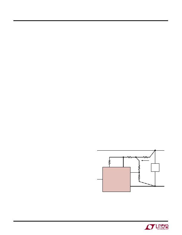
�Ground� pin� current� can� affect� regulation� as� shown� in�
�Figure� 2.� Parasitic� resistance� in� the� ground� pin� lead� will�
�create� a� voltage� drop� which� increases� output� voltage� as�
�load� current� is� increased.� Similarly,� output� voltage� can�
�decrease� as� input� voltage� increases� because� the� “I� OUT� /40”�
�component� of� ground� pin� current� drops� significantly� at�
�higher� input-output� differentials.� These� effects� are� small�
�enough� to� be� ignored� for� local� regulation� applications,� but�
�External� Current� Limit�
�The� LT1185� requires� a� resistor� to� set� current� limit.� The�
�+�
�PARASITIC�
�LEAD� RESISTANCES�
�–� r� b� +�
�r� a�
�+�
�value� of� this� resistor� is� 15k� divided� by� the� desired� current�
�limit� (in� amps).� The� resistor� for� 2A� current� limit� would� be�
�15k/2A� =� 7.5k.� Tolerance� over� temperature� is� ±� 10%,� so�
�current� limit� is� normally� set� 15%� above� maximum� load�
�current.� Foldback� limiting� can� be� employed� if� short-circuit�
�V� IN�
�–�
�V� IN�
�R� LIM�
�REF�
�LT1185�
�GND�
�FB�
�I� GND�
�R1*�
�2.37k�
�R2�
�LOAD�
�V� OUT�
�current� must� be� lower� than� full� load� current� (see� Typical�
�Applications).�
�V� OUT�
�–�
�The� LT1185� has� internal� current� limiting� which� will� over-�
�ride� external� current� limit� if� power� in� the� pass� transistor�
�is� excessive.� The� internal� limit� is� ≈� 3.6A� with� a� foldback�
�characteristic� which� is� dependent� on� input-output� volt-�
�age,� not� output� voltage� per� se� (see� Typical� Performace�
�Characteristics).�
�LT1185� ?� F02�
�*R1� SHOULD� BE� CONNECTED� DIRECTLY� TO� GROUND� LEAD,� NOT� TO� THE� LOAD,�
�SO� THAT� r� a� ≈� 0� ?� .� THIS� LIMITS� THE� OUTPUT� VOLTAGE� ERROR� TO� (I� GND� )(r� b� ).�
�ERRORS� CREATED� BY� r� a� ARE� MULTIPLIED� BY� (1� +� R2/R1).� NOTE� THAT� V� OUT�
�INCREASES� WITH� INCREASING� GROUND� PIN� CURRENT.� R2� SHOULD� BE� CONNECTED�
�DIRECTLY� TO� LOAD� FOR� REMOTE� SENSING�
�Figure� 2.� Proper� Connection� of� Positive� Sense� Lead�
�1185ff�
�8�
�相关PDF资料 |
PDF描述 |
|---|---|
| LT1085CT-3.3#PBF | IC REG LDO 3.3V 3A TO-220-3 |
| ADP1711AUJZ-0.9-R7 | IC REG LDO 0.9V .15A TSOT-23-5 |
| HMC15DREH-S93 | CONN EDGECARD 30POS .100 EYELET |
| GSC17DRTN-S13 | CONN EDGECARD 34POS .100 EXTEND |
| GMC17DRTN-S13 | CONN EDGECARD 34POS .100 EXTEND |
相关代理商/技术参数 |
参数描述 |
|---|---|
| LT1185IQ | 制造商:Linear Technology 功能描述:LDO Regulator Neg/Pos -2.5V to -25V2.5V to 25V 3A 6-Pin(5+Tab) DDPAK |
| LT1185IQ#PBF | 功能描述:IC REG LDO NEG ADJ 3A 5-DD RoHS:是 类别:集成电路 (IC) >> PMIC - 稳压器 - 线性 系列:- 标准包装:1 系列:- 稳压器拓扑结构:正,固定式 输出电压:8V 输入电压:10.5 V ~ 23 V 电压 - 压降(标准):1.7V @ 40mA 稳压器数量:1 电流 - 输出:100mA(最小值) 电流 - 限制(最小):- 工作温度:0°C ~ 125°C 安装类型:表面贴装 封装/外壳:8-SOIC(0.154",3.90mm 宽) 供应商设备封装:8-SOIC 包装:剪切带 (CT) 产品目录页面:1075 (CN2011-ZH PDF) 其它名称:296-24390-1 |
| LT1185IQ#PBF | 制造商:Linear Technology 功能描述:VOLTAGE REGULATOR LDO ADJ 3 制造商:Linear Technology 功能描述:VOLTAGE REGULATOR, LDO, ADJ, 3A, TO-263- |
| LT1185IQ#TR | 制造商:Linear Technology 功能描述:LDO Regulator Neg/Pos -2.5V to -25V2.5V to 25V 3A 6-Pin(5+Tab) DDPAK T/R |
| LT1185IQ#TRPBF | 功能描述:IC REG LDO NEG ADJ 3A 5-DD RoHS:是 类别:集成电路 (IC) >> PMIC - 稳压器 - 线性 系列:- 标准包装:1 系列:- 稳压器拓扑结构:正,固定式 输出电压:3V 输入电压:2.3 V ~ 5.5 V 电压 - 压降(标准):0.035V @ 150mA 稳压器数量:2 电流 - 输出:150mA 电流 - 限制(最小):300mA 工作温度:-40°C ~ 125°C 安装类型:表面贴装 封装/外壳:6-UFDFN 裸露焊盘,6-TMLF? 供应商设备封装:6-TMLF?(1.6x1.6) 包装:Digi-Reel® 产品目录页面:1104 (CN2011-ZH PDF) 其它名称:576-3018-6 |
发布紧急采购,3分钟左右您将得到回复。