- 您现在的位置:买卖IC网 > PDF目录15268 > LT1339CSW#TRPBF (Linear Technology)IC REG CTRLR BST PWM CM 20-SOIC PDF资料下载
参数资料
| 型号: | LT1339CSW#TRPBF |
| 厂商: | Linear Technology |
| 文件页数: | 12/20页 |
| 文件大小: | 0K |
| 描述: | IC REG CTRLR BST PWM CM 20-SOIC |
| 标准包装: | 1,000 |
| PWM 型: | 电流模式 |
| 输出数: | 1 |
| 频率 - 最大: | 150kHz |
| 占空比: | 90% |
| 电源电压: | 最高 60V |
| 降压: | 无 |
| 升压: | 是 |
| 回扫: | 无 |
| 反相: | 无 |
| 倍增器: | 无 |
| 除法器: | 无 |
| Cuk: | 无 |
| 隔离: | 无 |
| 工作温度: | 0°C ~ 70°C |
| 封装/外壳: | 20-SOIC(0.295",7.50mm 宽) |
| 包装: | 带卷 (TR) |
�� �
�
�LT1339�
�APPLICATIO� N� S� I� N� FOR� M� ATIO� N�
�the� converter� input� supply� is� enabled� with� no� voltage� on�
�the� LT1339� 12V� IN� pin,� the� LT1339� driver� output� clamps�
�will� not� be� activated.� To� prevent� turn-on,� an� external�
�current� path� must� be� used� to� bleed� off� charge� on� the�
�switch� MOSFET� gates.� High� value� bleed� resistors� (50k� to�
�250k)� should� be� connected� between� the� TG� and� SW� pins�
�and� between� BG� and� PGND.� This� provides� discharge� paths�
�for� the� switch� MOSFET� gates,� preventing� parasitic� turn-on�
�and� damage� to� the� MOSFETs.�
�Inductor� Selection�
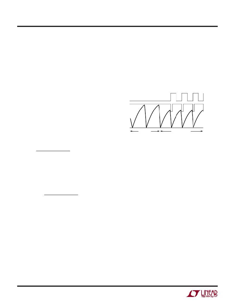
�Oscillator� Synchronization�
�The� LT1339� oscillator� generates� a� modified� sawtooth�
�waveform� at� the� C� T� pin� between� low� and� high� thresholds�
�of� about� 0.8V� (vl)� and� 2.5V� (vh)� respectively.� The� oscillator�
�can� be� synchronized� by� driving� a� TTL� level� pulse� into� the�
�SYNC� pin.� This� inputs� to� a� one-shot� circuit� that� reduces� the�
�oscillator� high� threshold� to� 2V� for� about� 200ns.� The� SYNC�
�input� signal� should� have� minimum� high/low� times� of� ≥� 1� μ� s.�
�SYNC�
�The� inductor� for� an� LT1339� converter� is� selected� based� on�
�output� power,� operating� frequency� and� efficiency� require-�
�ments.� Generally,� the� selection� of� inductor� value� can� be�
�2.5V�
�2V�
�(vh)�
�reduced� to� desired� maximum� ripple� current� in� the� inductor�
�(� ?� I).� For� a� buck� converter,� the� minimum� inductor� value� for�
�a� desired� maximum� operating� ripple� current� can� be� deter-�
�0.8V�
�FREE� RUN�
�SYNCHRONIZED�
�V� CT�
�(vl)�
�(� V� OUT� )� (� V� IN� ?� V� OUT� )�
�(� )(� I� ?� f� O� )(� V� IN� )�
�mined using the following relation:�
�L� MIN� =�
�Figure� 4.� Free� Run� and� Synchronized� Oscillator�
�Waveforms� (at� C� T� Pin)�
�Slope� Compensation�
�1339� F04�
�(� V� OUT� )� (� V� IN� ?� V� OUT� )�
�(� )(� )(� L� f� O� )(� V� IN� )�
�where f� O� = operating frequency. Given an inductor value�
�(L),� the� peak� inductor� current� is� the� sum� of� the� average�
�inductor� current� (I� AVG� )and� half� the� inductor� ripple� current�
�(� ?� I),� or:�
�I� PK� =� I� AVG� +�
�2�
�The� inductor� core� type� is� determined� by� peak� current� and�
�efficiency� requirements.� The� inductor� core� must� with-�
�stand� peak� current� without� saturating,� and� series� winding�
�resistance� and� core� losses� should� be� kept� as� small� as� is�
�practical� to� maximize� conversion� efficiency.�
�The� LT1339� peak� current� limit� threshold� is� 40%� greater� than�
�the� average� current� limit� threshold.� Slope� compensation�
�effects� reduce� this� margin� as� duty� cycle� increases.� This�
�margin� must� be� maintained� to� prevent� peak� current� limit�
�from� corrupting� the� programmed� value� for� average� current�
�limit.� Programming� the� peak� ripple� current� to� less� than� 15%�
�of� the� desired� average� current� limit� value� will� assure� porper�
�operation� of� the� average� current� limit� feature� through� 90%�
�duty� cycle� (see� Slope� Compensation� section).�
�12�
�Current� mode� switching� regulators� that� operate� with� a�
�duty� cycle� greater� than� 50%� and� have� continuous� inductor�
�current� can� exhibit� duty� cycle� instability.� While� a� regulator�
�will� not� be� damaged� and� may� even� continue� to� function�
�acceptably� during� this� type� of� subharmonic� oscillation,� an�
�irritating� high-pitched� squeal� is� usually� produced.�
�The� criterion� for� current� mode� duty� cycle� instability� is� met�
�when� the� increasing� slope� of� the� inductor� ripple� current� is�
�less� than� the� decreasing� slope,� which� is� the� case� at� duty�
�cycles� greater� than� 50%.� This� condition� is� illustrated� in�
�Figure� 5a.� The� inductor� ripple� current� starts� at� I� 1� ,� at� the�
�beginning� of� each� oscillator� switch� cycle.� Current�
�increases� at� a� rate� S1� until� the� current� reaches� the� control�
�trip� level� I� 2� .� The� controller� servo� loop� then� disables� the�
�main� switch� (and� enables� the� synchronous� switch)� and�
�inductor� current� begins� to� decrease� at� a� rate� S2.� If� the�
�current� switch� point� (I� 2� )� is� perturbed� slightly� and�
�increased� by� ?� I,� the� cycle� time� ends� such� that� the� mini-�
�mum� current� point� is� increased� by� a� factor� of� (1� +� S2/S1)�
�to� start� the� next� cycle.� On� each� successive� cycle,� this� error�
�is� multiplied� by� a� factor� of� S2/S1.� Therefore,� if� S2/S1� is�
�≥� 1,� the� system� is� unstable.�
�sn1339� 1339fas�
�相关PDF资料 |
PDF描述 |
|---|---|
| GSM24DSUN | CONN EDGECARD 48POS DIP .156 SLD |
| VE-274-EY-F4 | CONVERTER MOD DC/DC 48V 50W |
| LT1339CSW#TR | IC REG CTRLR BST PWM CM 20-SOIC |
| EMM12DWWN | CONN EDGECARD 24POS .156 SQ WW |
| ECM28DKKN | CONN EDGECARD 56POS .156 WW |
相关代理商/技术参数 |
参数描述 |
|---|---|
| LT1339I | 制造商:LINER 制造商全称:Linear Technology 功能描述:High Power Synchronous DC/DC Controller |
| LT1339IN | 功能描述:IC REG CTRLR BST PWM CM 20-DIP RoHS:否 类别:集成电路 (IC) >> PMIC - 稳压器 - DC DC 切换控制器 系列:- 标准包装:4,500 系列:PowerWise® PWM 型:控制器 输出数:1 频率 - 最大:1MHz 占空比:95% 电源电压:2.8 V ~ 5.5 V 降压:是 升压:无 回扫:无 反相:无 倍增器:无 除法器:无 Cuk:无 隔离:无 工作温度:-40°C ~ 125°C 封装/外壳:6-WDFN 裸露焊盘 包装:带卷 (TR) 配用:LM1771EVAL-ND - BOARD EVALUATION LM1771 其它名称:LM1771SSDX |
| LT1339IN#PBF | 功能描述:IC REG CTRLR BST PWM CM 20-DIP RoHS:是 类别:集成电路 (IC) >> PMIC - 稳压器 - DC DC 切换控制器 系列:- 标准包装:4,500 系列:PowerWise® PWM 型:控制器 输出数:1 频率 - 最大:1MHz 占空比:95% 电源电压:2.8 V ~ 5.5 V 降压:是 升压:无 回扫:无 反相:无 倍增器:无 除法器:无 Cuk:无 隔离:无 工作温度:-40°C ~ 125°C 封装/外壳:6-WDFN 裸露焊盘 包装:带卷 (TR) 配用:LM1771EVAL-ND - BOARD EVALUATION LM1771 其它名称:LM1771SSDX |
| LT1339ISW | 功能描述:IC REG CTRLR BST PWM CM 20-SOIC RoHS:否 类别:集成电路 (IC) >> PMIC - 稳压器 - DC DC 切换控制器 系列:- 标准包装:4,500 系列:PowerWise® PWM 型:控制器 输出数:1 频率 - 最大:1MHz 占空比:95% 电源电压:2.8 V ~ 5.5 V 降压:是 升压:无 回扫:无 反相:无 倍增器:无 除法器:无 Cuk:无 隔离:无 工作温度:-40°C ~ 125°C 封装/外壳:6-WDFN 裸露焊盘 包装:带卷 (TR) 配用:LM1771EVAL-ND - BOARD EVALUATION LM1771 其它名称:LM1771SSDX |
| LT1339ISW#PBF | 功能描述:IC REG CTRLR BST PWM CM 20-SOIC RoHS:是 类别:集成电路 (IC) >> PMIC - 稳压器 - DC DC 切换控制器 系列:- 特色产品:LM3753/54 Scalable 2-Phase Synchronous Buck Controllers 标准包装:1 系列:PowerWise® PWM 型:电压模式 输出数:1 频率 - 最大:1MHz 占空比:81% 电源电压:4.5 V ~ 18 V 降压:是 升压:无 回扫:无 反相:无 倍增器:无 除法器:无 Cuk:无 隔离:无 工作温度:-5°C ~ 125°C 封装/外壳:32-WFQFN 裸露焊盘 包装:Digi-Reel® 产品目录页面:1303 (CN2011-ZH PDF) 其它名称:LM3754SQDKR |
发布紧急采购,3分钟左右您将得到回复。