- 您现在的位置:买卖IC网 > PDF目录44980 > LT1377IS8#TRPBF (LINEAR TECHNOLOGY CORP) 2.7 A SWITCHING REGULATOR, 1160 kHz SWITCHING FREQ-MAX, PDSO8 PDF资料下载
参数资料
| 型号: | LT1377IS8#TRPBF |
| 厂商: | LINEAR TECHNOLOGY CORP |
| 元件分类: | 稳压器 |
| 英文描述: | 2.7 A SWITCHING REGULATOR, 1160 kHz SWITCHING FREQ-MAX, PDSO8 |
| 封装: | 0.150 INCH, PLASTIC, SO-8 |
| 文件页数: | 10/12页 |
| 文件大小: | 193K |
| 代理商: | LT1377IS8#TRPBF |
7
LT1372/LT1377
Positive fixed voltage versions are available (consult
Linear Technology marketing).
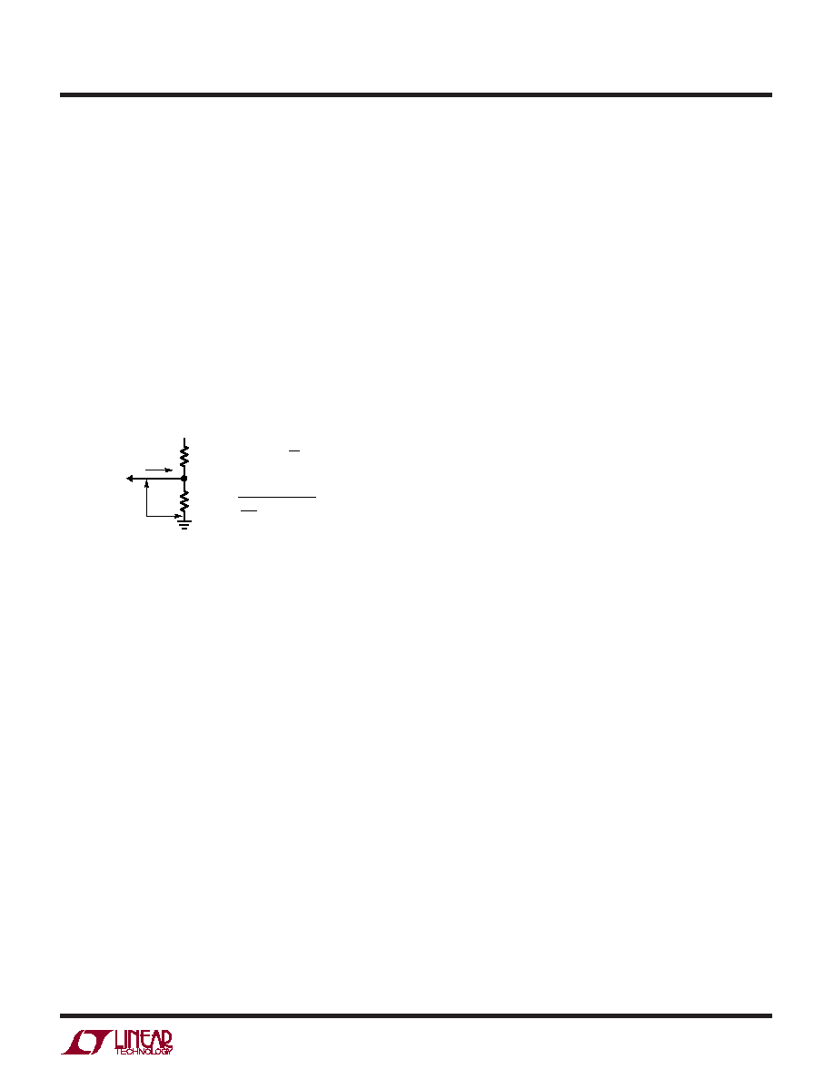
Negative Output Voltage Setting
The LT1372/LT1377 develops a – 2.49V reference (VNFR)
from the NFB pin to ground. Output voltage is set by
connecting the NFB pin to an output resistor divider
(Figure 2). The – 30
A NFB pin bias current (INFB) can
cause output voltage errors and should not be ignored.
This has been accounted for in the formula in Figure 2. The
suggested value for R2 is 2.49k. The FB pin is normally left
open for negative output application. See Dual Polarity
Output Voltage Sensing for limitatins on FB pin loading
when using the NFB pin.
Shutdown and Synchronization
The dual function S/S pin provides easy shutdown and
synchronization. It is logic level compatible and can be
pulled high, tied to VIN or left floating for normal operation.
A logic low on the S/S pin activates shutdown, reducing
the part’s supply current to 12
A. Typical synchronization
range is from 1.05 to 1.8 times the part’s natural switching
frequency, but is only guaranteed between 600kHz and
800kHz (LT1372) or 1.2MHz and 1.6MHz (LT1377). At
start-up, the synchronization signal should not be applied
until the feedback pin is above the frequency shift voltage
of 0.7V. If the NFB pin is used, synchronization should not
be applied until the NFB pin is more negative than – 1.4V.
A 12
s resetable shutdown delay network guarantees the
part will not go into shutdown while receiving a synchro-
nization signal.
Caution should be used when synchronizing above 700kHz
(LT1372) or 1.4MHz (LT1377) because at higher sync
frequencies the amplitude of the internal slope compensa-
tion used to prevent subharmonic switching is reduced.
This type of subharmonic switching only occurs when the
duty cycle of the switch is above 50%. Higher inductor
values will tend to eliminate problems.
Thermal Considerations
Care should be taken to ensure that the worst-case input
voltage and load current conditions do not cause exces-
sive die temperatures. The packages are rated at 120
°C/W
for SO (S8) and 130
°C/W for PDIP (N8).
Average supply current (including driver current) is:
IIN = 4mA + DC (ISW/60 + ISW × 0.004)
ISW = switch current
DC = switch duty cycle
Switch power dissipation is given by:
PSW = (ISW)2 × RSW × DC
RSW = output switch “On” resistance
Total power dissipation of the die is the sum of supply
current times supply voltage plus switch power:
PD(TOTAL) = (IIN × VIN) + PSW
Dual Polarity Output Voltage Sensing
Certain applications benefit from sensing both positive
and negative output voltages. One example is the “Dual
Output Flyback Converter with Overvoltage Protection”
circuit shown in the Typical Applications section. Each
output voltage resistor divider is individually set as de-
scribed above. When both the FB and NFB pins are used,
the LT1372/LT1377 acts to prevent either output from
going beyond its set output voltage. For example in this
application, if the positive output were more heavily loaded
than the negative, the negative output would be greater
and would regulate at the desired set-point voltage. The
positive output would sag slightly below its set-point
voltage. This technique prevents either output from going
unregulated high at no load. Please note that the load on
the FB pin should not exceed 250
A when the NFB pin is
used. This situation occurs when the resistor dividers are
used at
both FB and NFB. True load on FB is not the full
divider current unless the positive output is shorted to
ground. See Dual Output Flyback Converter application.
R1
–VOUT = VNFB
+ INFB (R1)
1 +
R2
LT1372 F02
NFB
PIN
VNFR
INFB
–VOUT
()R1
R2
R1 =
+ 30
× 10
–6
VOUT– 2.49
( ) (
)
2.49
R2
Figure 2. Negative Output Resistor Divider
APPLICATIO S I FOR ATIO
WU
UU
相关PDF资料 |
PDF描述 |
|---|---|
| LT1424CN8 | SWITCHING REGULATOR, 310 kHz SWITCHING FREQ-MAX, PDIP8 |
| LT1431MJ8#TRPBF | 1-OUTPUT TWO TERM VOLTAGE REFERENCE, 2.5 V, CDIP8 |
| LT1460BIN8-2.5#TRPBF | 1-OUTPUT THREE TERM VOLTAGE REFERENCE, 2.5 V, PDIP8 |
| LT1460EIN8-5#TRPBF | 1-OUTPUT THREE TERM VOLTAGE REFERENCE, 5 V, PDIP8 |
| LT1460DCN8-5#TRPBF | 1-OUTPUT THREE TERM VOLTAGE REFERENCE, 5 V, PDIP8 |
相关代理商/技术参数 |
参数描述 |
|---|---|
| LT1379HVIR#PBF | 制造商:LINTEC 功能描述: |
| LT137A | 制造商:LINER 制造商全称:Linear Technology 功能描述:Negative Adjustable Regulator |
| LT137A_1 | 制造商:LINER 制造商全称:Linear Technology 功能描述:Negative Adjustable Regulator |
| LT137AH | 制造商:LINER 制造商全称:Linear Technology 功能描述:Negative Adjustable Regulator |
| LT137AH/883B | 制造商:未知厂家 制造商全称:未知厂家 功能描述:Negative Adjustable Voltage Regulator |
发布紧急采购,3分钟左右您将得到回复。