- 您现在的位置:买卖IC网 > PDF目录44980 > LT1377IS8#TRPBF (LINEAR TECHNOLOGY CORP) 2.7 A SWITCHING REGULATOR, 1160 kHz SWITCHING FREQ-MAX, PDSO8 PDF资料下载
参数资料
| 型号: | LT1377IS8#TRPBF |
| 厂商: | LINEAR TECHNOLOGY CORP |
| 元件分类: | 稳压器 |
| 英文描述: | 2.7 A SWITCHING REGULATOR, 1160 kHz SWITCHING FREQ-MAX, PDSO8 |
| 封装: | 0.150 INCH, PLASTIC, SO-8 |
| 文件页数: | 8/12页 |
| 文件大小: | 193K |
| 代理商: | LT1377IS8#TRPBF |
5
LT1372/LT1377
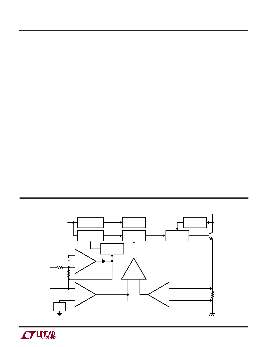
VC (Pin 1): The compensation pin is used for frequency
compensation, current limiting and soft start. It is the
output of the error amplifier and the input of the current
comparator. Loop frequency compensation can be per-
formed with an RC network connected from the VC pin to
ground.
FB (Pin 2): The feedback pin is used for positive output
voltage sensing and oscillator frequency shifting. It is the
inverting input to the error amplifier. The noninverting
input of this amplifier is internally tied to a 1.245V
reference. Load on the FB pin should not exceed 250
A
when the NFB pin is used. See Applications Information.
NFB (Pin 3): The negative feedback pin is used for negative
output voltage sensing. It is connected to the inverting
input of the negative feedback amplifier through a 100k
source resistor.
S/S (Pin 4): Shutdown and Synchronization Pin. The S/S
pin is logic level compatible. Shutdown is active low and
the shutdown threshold is typically 1.3V. For normal
operation, pull the S/S pin high, tie it to VIN or leave it
floating. To synchronize switching, drive the S/S pin be-
tween 600kHz and 800kHz (LT1372) or 1.2MHz to 1.6MHz
(LT1377).
VIN (Pin 5): Bypass input supply pin with 10F or more. The
part goes into undervoltage lockout when VIN drops below
2.5V. Undervoltage lockout stops switching and pulls the
VC pin low.
GND S (Pin 6): The ground sense pin is a “clean” ground.
The internal reference, error amplifier and negative feed-
back amplifier are referred to the ground sense pin. Con-
nect it to ground. Keep the ground path connection to the
output resistor divider and the VC compensation network
free of large ground currents.
GND (Pin 7): The ground pin is the emitter connection of
the power switch and has large currents flowing through it.
It should be connected directly to a good quality ground
plane.
VSW (Pin 8): The switch pin is the collector of the power
switch and has large currents flowing through it. Keep the
traces to the switching components as short as possible to
minimize radiation and voltage spikes.
–
+
NFBA
NFB
S/S
FB
100k
50k
0.08
–
+
EA
VC
VIN
GND
LT1372 BD
GND SENSE
1.245V
REF
5:1 FREQUENCY
SHIFT
OSC
SYNC
SHUTDOWN
DELAY AND RESET
LOW DROPOUT
2.3V REG
ANTI-SAT
LOGIC
DRIVER
SW
SWITCH
–
+
IA
AV ≈ 6
COMP
UU
U
PI FU CTIO S
BLOCK DIAGRA
W
相关PDF资料 |
PDF描述 |
|---|---|
| LT1424CN8 | SWITCHING REGULATOR, 310 kHz SWITCHING FREQ-MAX, PDIP8 |
| LT1431MJ8#TRPBF | 1-OUTPUT TWO TERM VOLTAGE REFERENCE, 2.5 V, CDIP8 |
| LT1460BIN8-2.5#TRPBF | 1-OUTPUT THREE TERM VOLTAGE REFERENCE, 2.5 V, PDIP8 |
| LT1460EIN8-5#TRPBF | 1-OUTPUT THREE TERM VOLTAGE REFERENCE, 5 V, PDIP8 |
| LT1460DCN8-5#TRPBF | 1-OUTPUT THREE TERM VOLTAGE REFERENCE, 5 V, PDIP8 |
相关代理商/技术参数 |
参数描述 |
|---|---|
| LT1379HVIR#PBF | 制造商:LINTEC 功能描述: |
| LT137A | 制造商:LINER 制造商全称:Linear Technology 功能描述:Negative Adjustable Regulator |
| LT137A_1 | 制造商:LINER 制造商全称:Linear Technology 功能描述:Negative Adjustable Regulator |
| LT137AH | 制造商:LINER 制造商全称:Linear Technology 功能描述:Negative Adjustable Regulator |
| LT137AH/883B | 制造商:未知厂家 制造商全称:未知厂家 功能描述:Negative Adjustable Voltage Regulator |
发布紧急采购,3分钟左右您将得到回复。