- 您现在的位置:买卖IC网 > PDF目录44980 > LT1377IS8#TRPBF (LINEAR TECHNOLOGY CORP) 2.7 A SWITCHING REGULATOR, 1160 kHz SWITCHING FREQ-MAX, PDSO8 PDF资料下载
参数资料
| 型号: | LT1377IS8#TRPBF |
| 厂商: | LINEAR TECHNOLOGY CORP |
| 元件分类: | 稳压器 |
| 英文描述: | 2.7 A SWITCHING REGULATOR, 1160 kHz SWITCHING FREQ-MAX, PDSO8 |
| 封装: | 0.150 INCH, PLASTIC, SO-8 |
| 文件页数: | 2/12页 |
| 文件大小: | 193K |
| 代理商: | LT1377IS8#TRPBF |
10
LT1372/LT1377
(magnetic) radiation is minimized by keeping output di-
ode, switch pin, and output bypass capacitor leads as
short as possible. E field radiation is kept low by minimiz-
ing the length and area of all traces connected to the switch
pin. A ground plane should always be used under the
switcher circuitry to prevent interplane coupling.
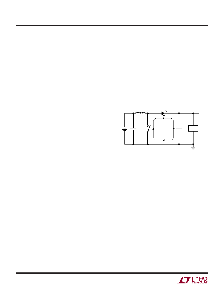
The high speed switching current path is shown schemati-
cally in Figure 3. Minimum lead length in this path is
essential to ensure clean switching and low EMI. The path
including the switch, output diode, and output capacitor is
the only one containing nanosecond rise and fall times.
Keep this path as short as possible.
LOAD
VOUT
L1
SWITCH
NODE
LT1372 F03
VIN
HIGH
FREQUENCY
CIRCULATING
PATH
Figure 3
More Help
For more detailed information on switching regulator
circuits, please see Application Note 19. Linear Technol-
ogy also offers a computer software program, SwitcherCAD,
to assist in designing switching converters. In addition,
our applications department is always ready to lend a
helping hand.
Frequency Compensation
Loop frequency compensation is performed on the output
of the error amplifier (VC pin) with a series RC network.
The main pole is formed by the series capacitor and the
output impedance (
≈500k) of the error amplifier. The
pole falls in the range of 2Hz to 20Hz. The series resistor
creates a “zero” at 1kHz to 5kHz, which improves loop
stability and transient response. A second capacitor,
typically one-tenth the size of the main compensation
capacitor, is sometimes used to reduce the switching
frequency ripple on the VC pin. VC pin ripple is caused by
output voltage ripple attenuated by the output divider and
multiplied by the error amplifier. Without the second
capacitor, VC pin ripple is:
VC Pin Ripple =
VRIPPLE = Output ripple (VP–P)
gm = Error amplifier transconductance
(
≈1500mho)
RC = Series resistor on VC pin
VOUT = DC output voltage
1.245(VRIPPLE)(gm)(RC)
(VOUT)
To prevent irregular switching, VC pin ripple should be
kept below 50mVP–P. Worst-case VC pin ripple occurs at
maximum output load current and will also be increased
if poor quality (high ESR) output capacitors are used. The
addition of a 0.0047
F capacitor on the VC pin reduces
switching frequency ripple to only a few millivolts. A low
value for RC will also reduce VC pin ripple, but loop phase
margin may be inadequate.
Switch Node Considerations
For maximum efficiency, switch rise and fall time are
made as short as possible. To prevent radiation and high
frequency resonance problems, proper layout of the com-
ponents connected to the switch node is essential. B field
APPLICATIO S I FOR ATIO
WU
UU
相关PDF资料 |
PDF描述 |
|---|---|
| LT1424CN8 | SWITCHING REGULATOR, 310 kHz SWITCHING FREQ-MAX, PDIP8 |
| LT1431MJ8#TRPBF | 1-OUTPUT TWO TERM VOLTAGE REFERENCE, 2.5 V, CDIP8 |
| LT1460BIN8-2.5#TRPBF | 1-OUTPUT THREE TERM VOLTAGE REFERENCE, 2.5 V, PDIP8 |
| LT1460EIN8-5#TRPBF | 1-OUTPUT THREE TERM VOLTAGE REFERENCE, 5 V, PDIP8 |
| LT1460DCN8-5#TRPBF | 1-OUTPUT THREE TERM VOLTAGE REFERENCE, 5 V, PDIP8 |
相关代理商/技术参数 |
参数描述 |
|---|---|
| LT1379HVIR#PBF | 制造商:LINTEC 功能描述: |
| LT137A | 制造商:LINER 制造商全称:Linear Technology 功能描述:Negative Adjustable Regulator |
| LT137A_1 | 制造商:LINER 制造商全称:Linear Technology 功能描述:Negative Adjustable Regulator |
| LT137AH | 制造商:LINER 制造商全称:Linear Technology 功能描述:Negative Adjustable Regulator |
| LT137AH/883B | 制造商:未知厂家 制造商全称:未知厂家 功能描述:Negative Adjustable Voltage Regulator |
发布紧急采购,3分钟左右您将得到回复。