- 您现在的位置:买卖IC网 > PDF目录13880 > LT1506CR#TRPBF (Linear Technology)IC REG BUCK ADJ 4.5A D2PAK PDF资料下载
参数资料
| 型号: | LT1506CR#TRPBF |
| 厂商: | Linear Technology |
| 文件页数: | 16/24页 |
| 文件大小: | 0K |
| 描述: | IC REG BUCK ADJ 4.5A D2PAK |
| 标准包装: | 750 |
| 类型: | 降压(降压) |
| 输出类型: | 可调式 |
| 输出数: | 1 |
| 输出电压: | 可调 |
| 输入电压: | 4 V ~ 15 V |
| PWM 型: | 电流模式 |
| 频率 - 开关: | 500kHz |
| 电流 - 输出: | 4.5A |
| 同步整流器: | 无 |
| 工作温度: | 0°C ~ 125°C |
| 安装类型: | 表面贴装 |
| 封装/外壳: | TO-263-8,D²Pak(7 引线+接片),TO-263CA |
| 包装: | 带卷 (TR) |
| 供应商设备封装: | D2PAK-7 |
�� �
�
�LT1506�
�APPLICATIO� N� S� I� N� FOR� M� ATIO� N�
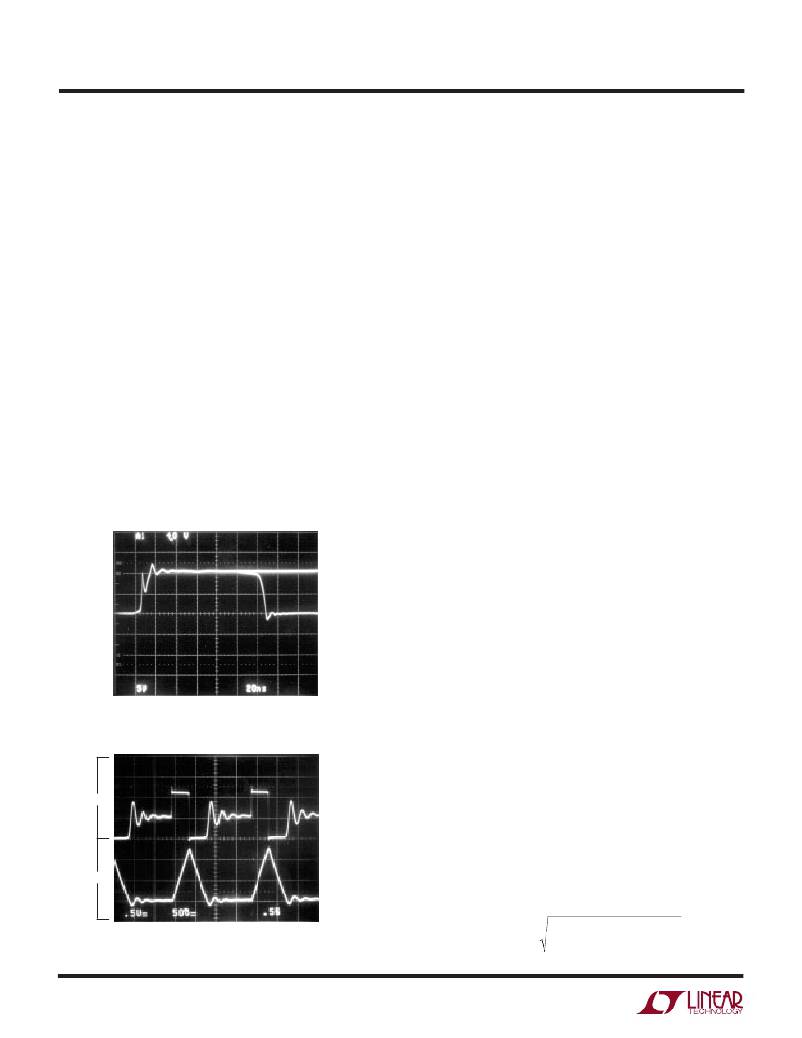
�PARASITIC� RESONANCE�
�Resonance� or� “ringing”� may� sometimes� be� seen� on� the�
�switch� node� (see� Figure� 7).� Very� high� frequency� ringing�
�following� switch� rise� time� is� caused� by� switch/diode/input�
�capacitor� lead� inductance� and� diode� capacitance.� Schot-�
�tky� diodes� have� very� high� “Q”� junction� capacitance� that�
�can� ring� for� many� cycles� when� excited� at� high� frequency.�
�If� total� lead� length� for� the� input� capacitor,� diode� and� switch�
�path� is� 1� inch,� the� inductance� will� be� approximately� 25nH.�
�At� switch� off,� this� will� produce� a� spike� across� the� NPN�
�output� device� in� addition� to� the� input� voltage.� At� higher�
�currents� this� spike� can� be� in� the� order� of� 10V� to� 20V� or�
�higher� with� a� poor� layout,� potentially� exceeding� the� abso-�
�lute� max� switch� voltage.� The� path� around� switch,� catch�
�diode� and� input� capacitor� must� be� kept� as� short� as�
�possible� to� ensure� reliable� operation.� When� looking� at� this,�
�a� >100MHz� oscilloscope� must� be� used,� and� waveforms�
�should� be� observed� on� the� leads� of� the� package.� This�
�switch� off� spike� will� also� cause� the� SW� node� to� go� below�
�ground.� The� LT1506� has� special� circuitry� inside� which�
�mitigates� this� problem,� but� negative� voltages� over� 1V�
�lasting� longer� than� 10ns� should� be� avoided.� Note� that�
�100MHz� oscilloscopes� are� barely� fast� enough� to� see� the�
�details� of� the� falling� edge� overshoot� in� Figure� 7.�
�A� second,� much� lower� frequency� ringing� is� seen� during�
�switch� off� time� if� load� current� is� low� enough� to� allow� the�
�inductor� current� to� fall� to� zero� during� part� of� the� switch� off�
�time� (see� Figure� 8).� Switch� and� diode� capacitance� reso-�
�nate� with� the� inductor� to� form� damped� ringing� at� 1MHz� to�
�10� MHz.� This� ringing� is� not� harmful� to� the� regulator� and� it�
�has� not� been� shown� to� contribute� significantly� to� EMI.� Any�
�attempt� to� damp� it� with� a� resistive� snubber� will� degrade�
�efficiency.�
�INPUT� BYPASSING� AND� VOLTAGE� RANGE�
�Input� Bypass� Capacitor�
�Step-down� converters� draw� current� from� the� input� supply�
�in� pulses.� The� average� height� of� these� pulses� is� equal� to�
�load� current,� and� the� duty� cycle� is� equal� to� V� OUT� /� V� IN� .� Rise�
�and� fall� time� of� the� current� is� very� fast.� A� local� bypass�
�capacitor� across� the� input� supply� is� necessary� to� ensure�
�proper� operation� of� the� regulator� and� minimize� the� ripple�
�5V/DIV�
�20ns/DIV�
�1375/76� F07�
�RISE� AND� FALL�
�WAVEFORMS� ARE�
�SUPERIMPOSED�
�(PULSE� WIDTH� IS�
�NOT� 120ns)�
�current� fed� back� into� the� input� supply.� The� capacitor� also�
�forces� switching� current� to� flow� in� a� tight� local� loop,�
�minimizing� EMI.�
�Do� not� cheat� on� the� ripple� current� rating� of� the� Input�
�bypass� capacitor,� but� also� don’t� get� hung� up� on� the� value�
�in� microfarads.� The� input� capacitor� is� intended� to� absorb�
�all� the� switching� current� ripple,� which� can� have� an� RMS�
�Figure� 7.� Switch� Node� Resonance�
�value� as� high� as� one� half� of� load� current.� Ripple� current�
�ratings� on� the� capacitor� must� be� observed� to� ensure�
�reliable� operation.� In� many� cases� it� is� necessary� to� parallel�
�two� capacitors� to� obtain� the� required� ripple� rating.� Both�
�(� )� /� V�
�I� RIPPLE� (� RMS� )� =� I� OUT� OUT� IN� OUT� IN�
�V� V� ?� V�
�5V/DIV�
�100mA/DIV�
�16�
�20ns/DIV� 1375/76� F11�
�0.5� μ� s/DIV� 1375/76� F08�
�Figure� 8.� Discontinuous� Mode� Ringing�
�SWITCH� NODE�
�VOLTAGE�
�INDUCTOR�
�CURRENT�
�capacitors� must� be� of� the� same� value� and� manufacturer� to�
�guarantee� power� sharing.� The� actual� value� of� the� capacitor�
�in� microfarads� is� not� particularly� important� because� at�
�500kHz,� any� value� above� 5� μ� F� is� essentially� resistive.� RMS�
�ripple� current� rating� is� the� critical� parameter.� Actual� RMS�
�current� can� be� calculated� from:�
�2�
�相关PDF资料 |
PDF描述 |
|---|---|
| MAX6758UTTD3+T | IC DETECT VOLT WINDOW SOT23-6 |
| GBB65DHND | CONN EDGECARD 130PS .050 DIP SLD |
| V375B3V3C100BG2 | CONVERTER MOD DC/DC 3.3V 100W |
| LT1374HVCS8#TRPBF | IC REG BUCK ADJ 4.5A 8SOIC |
| MAX6759UTRD0+T | IC DETECT VOLT WINDOW SOT23-6 |
相关代理商/技术参数 |
参数描述 |
|---|---|
| LT1506CS8 | 功能描述:IC REG BUCK ADJ 4.5A 8SOIC RoHS:否 类别:集成电路 (IC) >> PMIC - 稳压器 - DC DC 开关稳压器 系列:- 设计资源:Design Support Tool 标准包装:1 系列:- 类型:升压(升压) 输出类型:固定 输出数:1 输出电压:3V 输入电压:0.75 V ~ 2 V PWM 型:- 频率 - 开关:- 电流 - 输出:100mA 同步整流器:是 工作温度:-40°C ~ 85°C 安装类型:表面贴装 封装/外壳:SOT-23-5 细型,TSOT-23-5 包装:剪切带 (CT) 供应商设备封装:TSOT-23-5 其它名称:AS1323-BTTT-30CT |
| LT1506CS8#PBF | 功能描述:IC REG BUCK ADJ 4.5A 8SOIC RoHS:是 类别:集成电路 (IC) >> PMIC - 稳压器 - DC DC 开关稳压器 系列:- 标准包装:250 系列:- 类型:降压(降压) 输出类型:固定 输出数:1 输出电压:1.2V 输入电压:2.05 V ~ 6 V PWM 型:电压模式 频率 - 开关:2MHz 电流 - 输出:500mA 同步整流器:是 工作温度:-40°C ~ 85°C 安装类型:表面贴装 封装/外壳:6-UFDFN 包装:带卷 (TR) 供应商设备封装:6-SON(1.45x1) 产品目录页面:1032 (CN2011-ZH PDF) 其它名称:296-25628-2 |
| LT1506CS8#TR | 功能描述:IC REG BUCK ADJ 4.5A 8SOIC RoHS:否 类别:集成电路 (IC) >> PMIC - 稳压器 - DC DC 开关稳压器 系列:- 设计资源:Design Support Tool 标准包装:1 系列:- 类型:升压(升压) 输出类型:固定 输出数:1 输出电压:3V 输入电压:0.75 V ~ 2 V PWM 型:- 频率 - 开关:- 电流 - 输出:100mA 同步整流器:是 工作温度:-40°C ~ 85°C 安装类型:表面贴装 封装/外壳:SOT-23-5 细型,TSOT-23-5 包装:剪切带 (CT) 供应商设备封装:TSOT-23-5 其它名称:AS1323-BTTT-30CT |
| LT1506CS8#TRPBF | 功能描述:IC REG BUCK ADJ 4.5A 8SOIC RoHS:是 类别:集成电路 (IC) >> PMIC - 稳压器 - DC DC 开关稳压器 系列:- 设计资源:Design Support Tool 标准包装:1 系列:- 类型:升压(升压) 输出类型:固定 输出数:1 输出电压:3V 输入电压:0.75 V ~ 2 V PWM 型:- 频率 - 开关:- 电流 - 输出:100mA 同步整流器:是 工作温度:-40°C ~ 85°C 安装类型:表面贴装 封装/外壳:SOT-23-5 细型,TSOT-23-5 包装:剪切带 (CT) 供应商设备封装:TSOT-23-5 其它名称:AS1323-BTTT-30CT |
| LT1506CS8-3.3 | 功能描述:IC REG BUCK 3.3V 4.5A 8SOIC RoHS:否 类别:集成电路 (IC) >> PMIC - 稳压器 - DC DC 开关稳压器 系列:- 设计资源:Design Support Tool 标准包装:1 系列:- 类型:升压(升压) 输出类型:固定 输出数:1 输出电压:3V 输入电压:0.75 V ~ 2 V PWM 型:- 频率 - 开关:- 电流 - 输出:100mA 同步整流器:是 工作温度:-40°C ~ 85°C 安装类型:表面贴装 封装/外壳:SOT-23-5 细型,TSOT-23-5 包装:剪切带 (CT) 供应商设备封装:TSOT-23-5 其它名称:AS1323-BTTT-30CT |
发布紧急采购,3分钟左右您将得到回复。