- 您现在的位置:买卖IC网 > PDF目录13880 > LT1506CR#TRPBF (Linear Technology)IC REG BUCK ADJ 4.5A D2PAK PDF资料下载
参数资料
| 型号: | LT1506CR#TRPBF |
| 厂商: | Linear Technology |
| 文件页数: | 23/24页 |
| 文件大小: | 0K |
| 描述: | IC REG BUCK ADJ 4.5A D2PAK |
| 标准包装: | 750 |
| 类型: | 降压(降压) |
| 输出类型: | 可调式 |
| 输出数: | 1 |
| 输出电压: | 可调 |
| 输入电压: | 4 V ~ 15 V |
| PWM 型: | 电流模式 |
| 频率 - 开关: | 500kHz |
| 电流 - 输出: | 4.5A |
| 同步整流器: | 无 |
| 工作温度: | 0°C ~ 125°C |
| 安装类型: | 表面贴装 |
| 封装/外壳: | TO-263-8,D²Pak(7 引线+接片),TO-263CA |
| 包装: | 带卷 (TR) |
| 供应商设备封装: | D2PAK-7 |
�� �
�
�LT1506�
�APPLICATIO� N� S� I� N� FOR� M� ATIO� N�
�Redundant� Operation�
�The� circuit� shown� in� Figure� 15� is� fault� tolerant� when�
�operating� at� less� than� 8A� of� output� current.� If� one� device�
�fails,� the� output� will� remain� in� regulation.� The� feedback�
�loop� will� compensate� by� raising� the� voltage� on� the� V� C� pin,�
�increasing� switch� current� of� the� two� remaining� devices.�
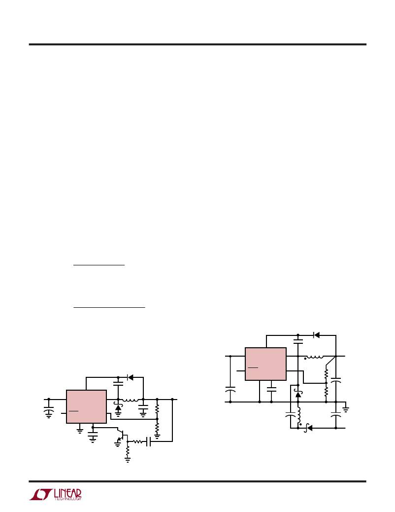
�BUCK� CONVERTER� WITH� ADJUSTABLE� SOFT� START�
�Large� capacitive� loads� can� cause� high� input� currents� at�
�start-up.� Figure� 16� shows� a� circuit� that� limits� the� dv/dt� of�
�the� output� at� start-up,� controlling� the� capacitor� charge�
�rate.� The� buck� converter� is� a� typical� configuration� with� the�
�addition� of� R3,� R4,� C� SS� and� Q1.� As� the� output� starts� to� rise,�
�Q1� turns� on,� regulating� switch� current� via� the� V� C� pin� to�
�maintain� a� constant� dv/dt� at� the� output.� Output� rise� time� is�
�controlled� by� the� current� through� C� SS� defined� by� R4� and�
�Q1’s� V� BE� .� Once� the� output� is� in� regulation,� Q1� turns� off� and�
�the� circuit� operates� normally.� R3� is� transient� protection� for�
�the� base� of� Q1.�
�output� current� is� unchanged.� Variants� of� this� circuit� can� be�
�used� for� sequencing� multiple� regulator� outputs.�
�Dual� Output� SEPIC� Converter�
�The� circuit� in� Figure� 17� generates� both� positive� and�
�negative� 5V� outputs� with� a� single� piece� of� magnetics.� The�
�two� inductors� shown� are� actually� just� two� windings� on� a�
�standard� B� H� Electronics� inductor.� The� topology� for� the� 5V�
�output� is� a� standard� buck� converter.� The� –� 5V� topology�
�would� be� a� simple� flyback� winding� coupled� to� the� buck�
�converter� if� C4� were� not� present.� C4� creates� a� SEPIC�
�(Single-Ended� Primary� Inductance� Converter)� topology�
�whicn� improves� regulation� and� reduces� ripple� current� in�
�L1.� Without� C4,� the� voltage� swing� on� L1B� compared� to�
�L1A� would� vary� due� to� relative� loading� and� coupling�
�losses.� C4� provides� a� low� impedance� path� to� maintain� an�
�equal� voltage� swing� in� L1B,� improving� regulation.� In� a�
�flyback� converter,� during� switch� on� time,� all� the� converter’s�
�energy� is� stroed� in� L1A� only,� since� no� current� flows� in� L1B.�
�At� switch� off,� energy� is� transferred� by� magnetic� coupling�
�RiseTime� =�
�(R 4)(C� SS� )( V� OUT� )�
�(� V� BE� )�
�into� L1B,� powering� the� –� 5V� rail.� C4� pulls� L1B� positive�
�during� switch� on� time,� causing� current� to� flow,� and� energy�
�to� build� in� L1B� and� C4.� At� switch� off,� the� energy� stored� in�
�RiseTime� =�
�Using the values shown in Figure 16,�
�(47 ? 10� 3� )(15 ? 10� –� 9� )(5)�
�0� .� 7�
�=� 5� ms�
�both� L1B� and� C4� supply� the� –5V� rail.� This� reduces� the�
�current� in� L1A� and� changes� L1B� current� waveform� from�
�square� to� triangular.� For� details� on� this� circuit� see� Design�
�Note� 100.�
�The� ramp� is� linear� and� rise� times� in� the� order� of� 100ms� are�
�D2�
�1N914�
�possible.� Since� the� circuit� is� voltage� controlled,� the� ramp�
�rate� is� unaffected� by� load� characteristics� and� maximum�
�INPUT�
�6V� TO� 15V�
�V� IN�
�BOOST�
�C2�
�0.27� μ� F�
�V� SW�
�L1*�
�6.8� μ� H�
�OUTPUT�
�5V�
�D2�
�LT1506�
�+�
�INPUT�
�12V�
�+�
�C3�
�10� μ� F�
�V� IN�
�SHDN�
�BOOST�
�LT1506�
�GND� V� C�
�C2�
�0.33� μ� F�
�V� SW�
�D1�
�FB�
�1N914�
�L1�
�5� μ� H�
�C1�
�100� μ� F�
�R1�
�5.36k�
�OUTPUT�
�5V�
�4A�
�GND�
�+�
�SHDN�
�GND�
�C3�
�10� μ� F�
�25V�
�CERAMIC�
�V� C�
�FB�
�C� C�
�1.5nF�
�C4**�
�4.7� μ� F�
�D1�
�L1*�
�R1�
�5.36k�
�R2�
�4.99k�
�C5**�
�100� μ� F�
�10V� TANT�
�+�
�+�
�C1**�
�100� μ� F�
�10V� TANT�
�C� C�
�1.5nF�
�Q1�
�C� SS�
�R3� 15nF�
�2k�
�R2�
�4.99k�
�*� L1� IS� A� SINGLE� CORE� WITH� TWO� WINDINGS�
�BH� ELECTRONICS� #501-0726�
�**� TOKIN� IE475ZY5U-C304�
�?� IF� LOAD� CAN� GO� TO� ZERO,� AN� OPTIONAL�
�D3�
�OUTPUT�
�–5V� ?�
�1506� F17�
�R4�
�47k�
�1506� F16�
�PRELOAD� OF� 1k� TO� 5k� MAY� BE� USED� TO�
�IMPROVE� LOAD� REGULATION�
�D1,� D3:� MBRD340�
�Figure� 16.� Buck� Converter� with� Adjustable� Soft� Start�
�Figure� 17.� Dual� Output� SEPIC� Converter�
�Information� furnished� by� Linear� Technology� Corporation� is� believed� to� be� accurate� and� reliable.�
�However,� no� responsibility� is� assumed� for� its� use.� Linear� Technology� Corporation� makes� no� represen-�
�tation� that� the� interconnection� of� its� circuits� as� described� herein� will� not� infringe� on� existing� patent� rights.�
�23�
�相关PDF资料 |
PDF描述 |
|---|---|
| MAX6758UTTD3+T | IC DETECT VOLT WINDOW SOT23-6 |
| GBB65DHND | CONN EDGECARD 130PS .050 DIP SLD |
| V375B3V3C100BG2 | CONVERTER MOD DC/DC 3.3V 100W |
| LT1374HVCS8#TRPBF | IC REG BUCK ADJ 4.5A 8SOIC |
| MAX6759UTRD0+T | IC DETECT VOLT WINDOW SOT23-6 |
相关代理商/技术参数 |
参数描述 |
|---|---|
| LT1506CS8 | 功能描述:IC REG BUCK ADJ 4.5A 8SOIC RoHS:否 类别:集成电路 (IC) >> PMIC - 稳压器 - DC DC 开关稳压器 系列:- 设计资源:Design Support Tool 标准包装:1 系列:- 类型:升压(升压) 输出类型:固定 输出数:1 输出电压:3V 输入电压:0.75 V ~ 2 V PWM 型:- 频率 - 开关:- 电流 - 输出:100mA 同步整流器:是 工作温度:-40°C ~ 85°C 安装类型:表面贴装 封装/外壳:SOT-23-5 细型,TSOT-23-5 包装:剪切带 (CT) 供应商设备封装:TSOT-23-5 其它名称:AS1323-BTTT-30CT |
| LT1506CS8#PBF | 功能描述:IC REG BUCK ADJ 4.5A 8SOIC RoHS:是 类别:集成电路 (IC) >> PMIC - 稳压器 - DC DC 开关稳压器 系列:- 标准包装:250 系列:- 类型:降压(降压) 输出类型:固定 输出数:1 输出电压:1.2V 输入电压:2.05 V ~ 6 V PWM 型:电压模式 频率 - 开关:2MHz 电流 - 输出:500mA 同步整流器:是 工作温度:-40°C ~ 85°C 安装类型:表面贴装 封装/外壳:6-UFDFN 包装:带卷 (TR) 供应商设备封装:6-SON(1.45x1) 产品目录页面:1032 (CN2011-ZH PDF) 其它名称:296-25628-2 |
| LT1506CS8#TR | 功能描述:IC REG BUCK ADJ 4.5A 8SOIC RoHS:否 类别:集成电路 (IC) >> PMIC - 稳压器 - DC DC 开关稳压器 系列:- 设计资源:Design Support Tool 标准包装:1 系列:- 类型:升压(升压) 输出类型:固定 输出数:1 输出电压:3V 输入电压:0.75 V ~ 2 V PWM 型:- 频率 - 开关:- 电流 - 输出:100mA 同步整流器:是 工作温度:-40°C ~ 85°C 安装类型:表面贴装 封装/外壳:SOT-23-5 细型,TSOT-23-5 包装:剪切带 (CT) 供应商设备封装:TSOT-23-5 其它名称:AS1323-BTTT-30CT |
| LT1506CS8#TRPBF | 功能描述:IC REG BUCK ADJ 4.5A 8SOIC RoHS:是 类别:集成电路 (IC) >> PMIC - 稳压器 - DC DC 开关稳压器 系列:- 设计资源:Design Support Tool 标准包装:1 系列:- 类型:升压(升压) 输出类型:固定 输出数:1 输出电压:3V 输入电压:0.75 V ~ 2 V PWM 型:- 频率 - 开关:- 电流 - 输出:100mA 同步整流器:是 工作温度:-40°C ~ 85°C 安装类型:表面贴装 封装/外壳:SOT-23-5 细型,TSOT-23-5 包装:剪切带 (CT) 供应商设备封装:TSOT-23-5 其它名称:AS1323-BTTT-30CT |
| LT1506CS8-3.3 | 功能描述:IC REG BUCK 3.3V 4.5A 8SOIC RoHS:否 类别:集成电路 (IC) >> PMIC - 稳压器 - DC DC 开关稳压器 系列:- 设计资源:Design Support Tool 标准包装:1 系列:- 类型:升压(升压) 输出类型:固定 输出数:1 输出电压:3V 输入电压:0.75 V ~ 2 V PWM 型:- 频率 - 开关:- 电流 - 输出:100mA 同步整流器:是 工作温度:-40°C ~ 85°C 安装类型:表面贴装 封装/外壳:SOT-23-5 细型,TSOT-23-5 包装:剪切带 (CT) 供应商设备封装:TSOT-23-5 其它名称:AS1323-BTTT-30CT |
发布紧急采购,3分钟左右您将得到回复。