参数资料
| 型号: | LT1676IS8#TRPBF |
| 厂商: | Linear Technology |
| 文件页数: | 5/16页 |
| 文件大小: | 0K |
| 描述: | IC REG BUCK ADJ 0.7A 8SOIC |
| 标准包装: | 2,500 |
| 类型: | 降压(降压) |
| 输出类型: | 可调式 |
| 输出数: | 1 |
| 输出电压: | 1.24 V ~ 51 V |
| 输入电压: | 7.4 V ~ 60 V |
| PWM 型: | 电流模式,混合 |
| 频率 - 开关: | 100kHz |
| 电流 - 输出: | 700mA |
| 同步整流器: | 无 |
| 工作温度: | -40°C ~ 125°C |
| 安装类型: | 表面贴装 |
| 封装/外壳: | 8-SOIC(0.154",3.90mm 宽) |
| 包装: | 带卷 (TR) |
| 供应商设备封装: | 8-SOIC |
�� �
�
�LT1676�
�PI� N� FU� N� CTIO� N� S�
�SHDN� (Pin� 1):� When� pulled� below� the� shutdown� mode�
�threshold,� nominally� 0.30V,� this� pin� turns� off� the� regula-�
�tor� and� reduces� V� IN� input� current� to� a� few� tens� of� micro-�
�amperes� (shutdown� mode).�
�When� this� pin� is� held� above� the� shutdown� mode� thresh-�
�old,� but� below� the� lockout� threshold,� the� part� will� be�
�operational� with� the� exception� that� output� switching�
�action� will� be� inhibited� (lockout� mode).� A� user-adjustable�
�undervoltage� lockout� can� be� implemented� by� driving� this�
�pin� from� an� external� resistor� divider� to� V� IN� .� This� action� is�
�logically� “ANDed”� with� the� internal� UVLO,� set� at� nominally�
�6.7V,� such� that� minimum� V� IN� can� be� increased� above�
�6.7V,� but� not� decreased� (see� Applications� Information).�
�If� unused,� this� pin� should� be� left� open.� However,� the� high�
�impedance� nature� of� this� pin� renders� it� susceptible� to�
�coupling� from� the� high� speed� V� SW� node,� so� a� small�
�capacitor� to� ground,� typically� 100pF� or� so� is� recom-�
�mended� when� the� pin� is� left� “open.”�
�V� CC� (Pin� 2):� This� pin� is� used� to� power� the� internal� control�
�circuitry� off� of� the� switching� supply� output.� Proper� use� of�
�this� pin� enhances� overall� power� supply� efficiency.� During�
�start-up� conditions,� internal� control� circuitry� is� powered�
�directly� from� V� IN� .� If� the� output� capacitor� is� located� more�
�than� an� inch� from� the� V� CC� pin,� a� separate� 0.1� μ� F� bypass�
�capacitor� to� ground� may� be� required� right� at� the� pin.�
�V� SW� (Pin� 3):� This� is� the� emitter� node� of� the� output� switch�
�and� has� large� currents� flowing� through� it.� This� node�
�moves� at� a� high� dV/dt� rate,� especially� when� in� “boost”�
�mode.� Keep� the� traces� to� the� switching� components� as�
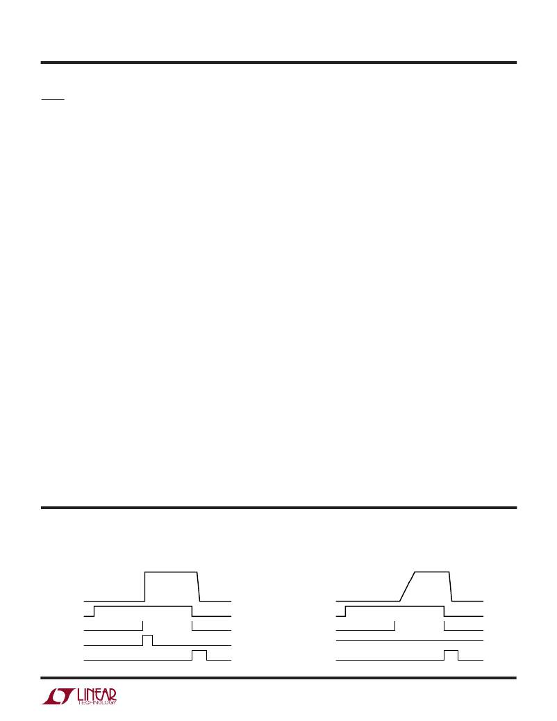
�TI� M� I� N� G� DIAGRA� M� S�
�High� dV/dt� Mode�
�V� IN�
�V� SW�
�0�
�SWDR�
�SWON�
�BOOST�
�SWOFF�
�1676� TD01�
�short� as� possible� to� minimize� electromagnetic� radiation�
�and� voltage� spikes.�
�GND� (Pin� 4):� This� is� the� device� ground� pin.� The� internal�
�reference� and� feedback� amplifier� are� referred� to� it.� Keep�
�the� ground� path� connection� to� the� FB� divider� and� the� V� C�
�compensation� capacitor� free� of� large� ground� currents.�
�V� IN� (Pin� 5):� This� is� the� high� voltage� supply� pin� for� the�
�output� switch.� It� also� supplies� power� to� the� internal� control�
�circuitry� during� start-up� conditions� or� if� the� V� CC� pin� is� left�
�open.� A� high� quality� bypass� capacitor� that� meets� the� input�
�ripple� current� requirements� is� needed� here.� (See� Applica-�
�tions� Information.)�
�SYNC� (Pin� 6):� Pin� used� to� synchronize� internal� oscillator�
�to� the� external� frequency� reference.� It� is� directly� logic�
�compatible� and� can� be� driven� with� any� signal� between�
�10%� and� 90%� duty� cycle.� The� sync� function� is� internally�
�disabled� if� the� FB� pin� voltage� is� low� enough� to� cause�
�oscillator� slowdown.� If� unused,� this� pin� should� be� grounded.�
�FB� (Pin� 7):� This� is� the� inverting� input� to� the� feedback�
�amplifier.� The� noninverting� input� of� this� amplifier� is� inter-�
�nally� tied� to� the� 1.24V� reference.� This� pin� also� slows� down�
�the� frequency� of� the� internal� oscillator� when� its� voltage� is�
�abnormally� low,� e.g.,� 2/3� of� normal� or� less.� This� feature�
�helps� maintain� proper� short-circuit� protection.�
�V� C� (Pin� 8):� This� is� the� control� voltage� pin� which� is� the�
�output� of� the� feedback� amplifier� and� the� input� of� the�
�current� comparator.� Frequency� compensation� of� the� over-�
�all� loop� is� effected� by� placing� a� capacitor,� (or� in� most� cases�
�a� series� RC� combination)� between� this� node� and� ground.�
�Low� dV/dt� Mode�
�V� IN�
�V� SW�
�0�
�SWDR�
�SWON�
�BOOST�
�SWOFF�
�1676� TD02�
�5�
�相关PDF资料 |
PDF描述 |
|---|---|
| LT1680ISW#PBF | IC REG CTRLR BST PWM CM 16-SOIC |
| LT1683EG#PBF | IC REG CTRLR PWM CM 20-SSOP |
| LT1725IGN#TR | IC REG CTRLR FLYBK ISO CM 16SSOP |
| LT1737IGN#PBF | IC REG CTRLR FLYBK ISO CM 16SSOP |
| LT1738EG#PBF | IC REG CTRLR PWM CM 20-SSOP |
相关代理商/技术参数 |
参数描述 |
|---|---|
| LT1677 | 制造商:LINER 制造商全称:Linear Technology 功能描述:Low Noise, Rail-to-Rail Precision Op Amp |
| LT1677_1 | 制造商:LINER 制造商全称:Linear Technology 功能描述:Low Noise, Rail-to-Rail Precision Op Amp |
| LT1677C | 制造商:LINER 制造商全称:Linear Technology 功能描述:Low Noise, Rail-to-Rail Precision Op Amp |
| LT1677CN8 | 功能描述:IC OPAMP R-R I/O SGL LN 8DIP RoHS:否 类别:集成电路 (IC) >> Linear - Amplifiers - Instrumentation 系列:- 标准包装:50 系列:- 放大器类型:通用 电路数:2 输出类型:满摆幅 转换速率:1.8 V/µs 增益带宽积:6.5MHz -3db带宽:4.5MHz 电流 - 输入偏压:5nA 电压 - 输入偏移:100µV 电流 - 电源:65µA 电流 - 输出 / 通道:35mA 电压 - 电源,单路/双路(±):1.8 V ~ 5.25 V,±0.9 V ~ 2.625 V 工作温度:-40°C ~ 85°C 安装类型:表面贴装 封装/外壳:10-TFSOP,10-MSOP(0.118",3.00mm 宽) 供应商设备封装:10-MSOP 包装:管件 |
| LT1677CN8#PBF | 功能描述:IC OPAMP R-R I/O SGL LN 8DIP RoHS:是 类别:集成电路 (IC) >> Linear - Amplifiers - Instrumentation 系列:- 标准包装:50 系列:- 放大器类型:通用 电路数:2 输出类型:满摆幅 转换速率:1.8 V/µs 增益带宽积:6.5MHz -3db带宽:4.5MHz 电流 - 输入偏压:5nA 电压 - 输入偏移:100µV 电流 - 电源:65µA 电流 - 输出 / 通道:35mA 电压 - 电源,单路/双路(±):1.8 V ~ 5.25 V,±0.9 V ~ 2.625 V 工作温度:-40°C ~ 85°C 安装类型:表面贴装 封装/外壳:10-TFSOP,10-MSOP(0.118",3.00mm 宽) 供应商设备封装:10-MSOP 包装:管件 |
发布紧急采购,3分钟左右您将得到回复。