参数资料
| 型号: | LT1676IS8#TRPBF |
| 厂商: | Linear Technology |
| 文件页数: | 9/16页 |
| 文件大小: | 0K |
| 描述: | IC REG BUCK ADJ 0.7A 8SOIC |
| 标准包装: | 2,500 |
| 类型: | 降压(降压) |
| 输出类型: | 可调式 |
| 输出数: | 1 |
| 输出电压: | 1.24 V ~ 51 V |
| 输入电压: | 7.4 V ~ 60 V |
| PWM 型: | 电流模式,混合 |
| 频率 - 开关: | 100kHz |
| 电流 - 输出: | 700mA |
| 同步整流器: | 无 |
| 工作温度: | -40°C ~ 125°C |
| 安装类型: | 表面贴装 |
| 封装/外壳: | 8-SOIC(0.154",3.90mm 宽) |
| 包装: | 带卷 (TR) |
| 供应商设备封装: | 8-SOIC |
�� �
�
�LT1676�
�APPLICATIO� N� S� I� N� FOR� M� ATIO� N�
�f� ?� t� ON� ≤� F�
�whichtantalumcapacitorsaregenerallyunavailable.Rela-�
�tively� bulky� “high� frequency”� aluminum� electrolytic� types,�
�specifically� constructed� and� rated� for� switching� supply�
�applications,� may� be� the� only� choice.�
�Minimum� Load� Considerations�
�As� discussed� previously,� a� lightly� loaded� LT1676� with� V� C�
�pin� control� voltage� below� the� boost� threshold� will� operate�
�in� low� dV/dt� mode.� This� affords� greater� controllability� at�
�light� loads,� as� minimum� t� ON� requirements� are� relaxed.� In�
�many� applications,� it� is� possible� to� operate� the� LT1676�
�down� to� zero� external� load� without� “pulse� skipping”!�
�In� these� cases,� the� LT1676’s� modest� V� CC� current�
�requirement� of� several� milliamperes� provides� enough� of� a�
�load� to� avoid� pulse� skipping.�
�However,� some� users� may� be� indifferent� to� pulse� skipping�
�behavior,� but� instead� may� be� concerned� with� maintaining�
�maximum� possible� efficiency� at� light� loads.� This� require-�
�ment� can� be� satisfied� by� forcing� the� part� into� Burst� Mode� TM�
�operation.� The� use� of� an� external� comparator� whose�
�output� controls� the� shutdown� pin� allows� high� efficiency� at�
�light� loads� through� Burst� Mode� operation� behavior� (see�
�Typical� Applications� and� Figure� 8).�
�Maximum� Load/Short-Circuit� Considerations�
�The� LT1676� is� a� current� mode� controller.� It� uses� the� V� C�
�node� voltage� as� an� input� to� a� current� comparator� which�
�turns� off� the� output� switch� on� a� cycle-by-cycle� basis� as�
�this� peak� current� is� reached.� The� internal� clamp� on� the� V� C�
�node,� nominally� 2V,� then� acts� as� an� output� switch� peak�
�current� limit.� This� action� becomes� the� switch� current� limit�
�specification.� The� maximum� available� output� power� is�
�t� ON(MIN)� .� When� combined� with� the� large� ratio� of� V� IN� to�
�(V� F� +� I� ?� R),� the� diode� forward� voltage� plus� inductor� I� ?� R�
�voltage� drop,� the� potential� exists� for� a� loss� of� control.�
�Expressed� mathematically� the� requirement� to� maintain�
�control� is:�
�V� +� I ? R�
�V� IN�
�where:�
�f� =� switching� frequency�
�t� ON� =� switch� ON� time�
�V� F� =� diode� forward� voltage�
�V� IN� =� Input� voltage�
�I� ?� R� =� inductor� I� ?� R� voltage� drop�
�If� this� condition� is� not� observed,� the� current� will� not� be�
�limited� at� I� PK� ,� but� will� cycle-by-cycle� ratchet� up� to� some�
�higher� value.� Using� the� nominal� LT1676� clock� frequency�
�of� 100KHz,� a� V� IN� of� 48V� and� a� (V� F� +� I� ?� R)� of� say� 0.7V,� the�
�maximum� t� ON� to� maintain� control� would� be� approximately�
�140ns,� an� unacceptably� short� time.�
�The� solution� to� this� dilemma� is� to� slow� down� the� oscillator�
�when� the� FB� pin� voltage� is� abnormally� low� thereby� indicat-�
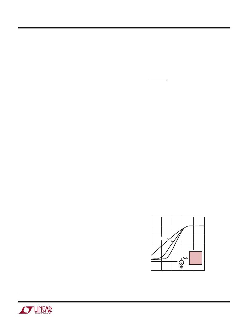
�ing� some� sort� of� short-circuit� condition.� Figure� 2� shows�
�the� typical� response� of� Oscillator� Frequency� vs� FB� divider�
�Thevenin� voltage� and� impedance.� Oscillator� frequency� is�
�unaffected� until� FB� voltage� drops� to� about� 2/3� of� its� normal�
�value.� Below� this� point� the� oscillator� frequency� decreases�
�roughly� linearly� down� to� a� limit� of� about� 25kHz.� This� lower�
�120�
�100�
�then� determined� by� the� switch� current� limit.�
�80�
�R� TH� = 22k�
�A� potential� controllability� problem� could� occur� under�
�short-circuit� conditions.� If� the� power� supply� output� is�
�60�
�R� TH� = 10k�
�R� TH� = 4.7k�
�short� circuited,� the� feedback� amplifier� responds� to� the� low�
�output� voltage� by� raising� the� control� voltage,� V� C� ,� to� its�
�peak� current� limit� value.� Ideally,� the� output� switch� would�
�40�
�20�
�R� TH�
�LT1676�
�FB�
�be� turned� on,� and� then� turned� off� as� its� current� exceeded�
�the� value� indicated� by� V� C� .� However,� there� is� finite� response�
�0�
�0�
�0.25� 0.50� 0.75� 1.00�
�FB� DIVIDER� THEVENIN� VOLTAGE� (V)�
�1.25�
�time� involved� in� both� the� current� comparator� and� turnoff�
�of� the� output� switch.� These� result� in� a� minimum� on� time�
�Burst� Mode� is� a� trademark� of� Linear� Technology� Corporation.�
�1676� F02�
�Figure� 2.� Oscillator� Frequency� vs� FB� Divider�
�Thevenin� Voltage� and� Impedance�
�9�
�相关PDF资料 |
PDF描述 |
|---|---|
| LT1680ISW#PBF | IC REG CTRLR BST PWM CM 16-SOIC |
| LT1683EG#PBF | IC REG CTRLR PWM CM 20-SSOP |
| LT1725IGN#TR | IC REG CTRLR FLYBK ISO CM 16SSOP |
| LT1737IGN#PBF | IC REG CTRLR FLYBK ISO CM 16SSOP |
| LT1738EG#PBF | IC REG CTRLR PWM CM 20-SSOP |
相关代理商/技术参数 |
参数描述 |
|---|---|
| LT1677 | 制造商:LINER 制造商全称:Linear Technology 功能描述:Low Noise, Rail-to-Rail Precision Op Amp |
| LT1677_1 | 制造商:LINER 制造商全称:Linear Technology 功能描述:Low Noise, Rail-to-Rail Precision Op Amp |
| LT1677C | 制造商:LINER 制造商全称:Linear Technology 功能描述:Low Noise, Rail-to-Rail Precision Op Amp |
| LT1677CN8 | 功能描述:IC OPAMP R-R I/O SGL LN 8DIP RoHS:否 类别:集成电路 (IC) >> Linear - Amplifiers - Instrumentation 系列:- 标准包装:50 系列:- 放大器类型:通用 电路数:2 输出类型:满摆幅 转换速率:1.8 V/µs 增益带宽积:6.5MHz -3db带宽:4.5MHz 电流 - 输入偏压:5nA 电压 - 输入偏移:100µV 电流 - 电源:65µA 电流 - 输出 / 通道:35mA 电压 - 电源,单路/双路(±):1.8 V ~ 5.25 V,±0.9 V ~ 2.625 V 工作温度:-40°C ~ 85°C 安装类型:表面贴装 封装/外壳:10-TFSOP,10-MSOP(0.118",3.00mm 宽) 供应商设备封装:10-MSOP 包装:管件 |
| LT1677CN8#PBF | 功能描述:IC OPAMP R-R I/O SGL LN 8DIP RoHS:是 类别:集成电路 (IC) >> Linear - Amplifiers - Instrumentation 系列:- 标准包装:50 系列:- 放大器类型:通用 电路数:2 输出类型:满摆幅 转换速率:1.8 V/µs 增益带宽积:6.5MHz -3db带宽:4.5MHz 电流 - 输入偏压:5nA 电压 - 输入偏移:100µV 电流 - 电源:65µA 电流 - 输出 / 通道:35mA 电压 - 电源,单路/双路(±):1.8 V ~ 5.25 V,±0.9 V ~ 2.625 V 工作温度:-40°C ~ 85°C 安装类型:表面贴装 封装/外壳:10-TFSOP,10-MSOP(0.118",3.00mm 宽) 供应商设备封装:10-MSOP 包装:管件 |
发布紧急采购,3分钟左右您将得到回复。