- 您现在的位置:买卖IC网 > PDF目录377712 > LT1720CMS8 (LINEAR TECHNOLOGY CORP) Dual/Quad, 4.5ns, Single Supply 3V/5V Comparators with Rail-to-Rail Outputs PDF资料下载
参数资料
| 型号: | LT1720CMS8 |
| 厂商: | LINEAR TECHNOLOGY CORP |
| 元件分类: | 运动控制电子 |
| 英文描述: | Dual/Quad, 4.5ns, Single Supply 3V/5V Comparators with Rail-to-Rail Outputs |
| 中文描述: | DUAL COMPARATOR, 4500 uV OFFSET-MAX, 7 ns RESPONSE TIME, PDSO8 |
| 封装: | PLASTIC, MSOP-8 |
| 文件页数: | 9/28页 |
| 文件大小: | 317K |
| 代理商: | LT1720CMS8 |
第1页第2页第3页第4页第5页第6页第7页第8页当前第9页第10页第11页第12页第13页第14页第15页第16页第17页第18页第19页第20页第21页第22页第23页第24页第25页第26页第27页第28页
9
LT1720/LT1721
The exact amount of hysteresis will vary from part to part
as indicated in the specifications table. The hysteresis level
will also vary slightly with changes in supply voltage and
common mode voltage. A key advantage of the LT1720/
LT1721 is the significant reduction in these effects, which
is important whenever an LT1720/LT1721 is used to de-
tect a threshold crossing in one direction only. In such a
case, the relevant trip point will be all that matters, and a
stable offset voltage with an unpredictable level of hyster-
esis, as seen in competing comparators, is of little value.
The LT1720/LT1721 are many times better than prior com-
parators in these regards. In fact, the CMRR and PSRR
tests are performed by checking for changes in either trip
point to the limits indicated in the specifications table.
Because the offset voltage is the average of the trip points,
the CMRR and PSRR of the offset voltage is therefore
guaranteed to be at least as good as those limits. This
more stringent test also puts a limit on the common mode
and power supply dependence of the hysteresis voltage.
Additional hysteresis may be added externally. The rail-to-
rail outputs of the LT1720/LT1721 make this more pre-
dictable than with TTL output comparators due to the
LT1720/LT1721’s small variability of V
OH
(output high
voltage).
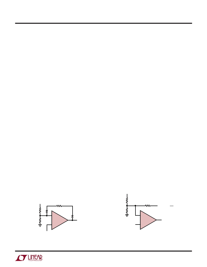
To add additional hysteresis, set up positive feedback by
adding additional external resistor R3 as shown in Figure
3. Resistor R3 adds a portion of the output to the threshold
set by the resistor string. The LT1720/LT1721 pulls the
outputs to the supply rail and ground to within 200mV of
the rails with light loads, and to within 400mV with heavy
loads. For the load of most circuits, a good model for the
APPLICATIO
S I
FOR
ATIO
U
W
U
U
Figure 4. Model for Additional Hysteresis Calculations
–
+
1/2 LT1720
1720/21 F04
R2
′
V
REF
V
TH
R3
V
CC
2
V
AVERAGE
=
R1
voltage on the right side of R3 is 300mV or V
CC
– 300mV,
for a total voltage swing of (V
CC
– 300mV) – 300mV =
V
CC
– 600mV.
With this in mind, calculation of the resistor values needed
is a two-step process. First, calculate the value of R3 based
on the additional hysteresis desired, the output voltage
swing, and the impedance of the primary bias string:
R3 = (R1
R2)(V
CC
– 0.6V)/(additional hysteresis)
Additional hysteresis is the desired overall hysteresis less
the internal 3.5mV hysteresis.
The second step is to recalculate R2 to set the same
average threshold as before. The average threshold before
was set at V
TH
= (V
REF
)(R1)/(R1 + R2). The new R2 is
calculated based on the average output voltage (V
CC
/2)
and the simplified circuit model in Figure 4. To assure that
the comparator’s noninverting input is, on average, the
same V
TH
as before:
R2
′
= (V
REF
– V
TH
)/(V
TH
/R1 + (V
TH
– V
CC
/2)/R3)
For additional hysteresis of 10mV or less, it is not uncom-
mon for R2
′
to be the same as R2 within 1% resistor
tolerances.
This method will work for additional hysteresis of up to a
few hundred millivolts. Beyond that, the impedance of R3
is low enough to effect the bias string, and adjustment of
R1 may also be required. Note that the currents through
the R1/R2 bias string should be many times the input
currents of the LT1720/LT1721. For 5% accuracy, the
current must be at least 120
μ
A(6
μ
A I
B
÷
0.05); more for
higher accuracy.
Figure 3. Additional External Hysteresis
–
+
1/2 LT1720
INPUT
1720/21 F03
R2
V
REF
R3
R1
相关PDF资料 |
PDF描述 |
|---|---|
| LT1721IS | Dual/Quad, 4.5ns, Single Supply 3V/5V Comparators with Rail-to-Rail Outputs |
| LT1722 | Single, Dual, Quad 200MHz Low Noise Precision Op Amps |
| LT1723CMS8 | Single, Dual, Quad 200MHz Low Noise Precision Op Amps |
| LT1723CS8 | Single, Dual, Quad 200MHz Low Noise Precision Op Amps |
| LT1723IMS8 | Single, Dual, Quad 200MHz Low Noise Precision Op Amps |
相关代理商/技术参数 |
参数描述 |
|---|---|
| LT1720CMS8#PBF | 功能描述:IC COMP R-RINOUT DUAL 8-MSOP RoHS:是 类别:集成电路 (IC) >> 线性 - 比较器 系列:UltraFast™ 标准包装:1 系列:- 类型:通用 元件数:1 输出类型:CMOS,开路集电极,TTL 电压 - 电源,单路/双路(±):2.7 V ~ 5.5 V 电压 - 输入偏移(最小值):7mV @ 5V 电流 - 输入偏压(最小值):0.25µA @ 5V 电流 - 输出(标准):84mA @ 5V 电流 - 静态(最大值):120µA CMRR, PSRR(标准):- 传输延迟(最大):600ns 磁滞:- 工作温度:-40°C ~ 85°C 封装/外壳:SC-74A,SOT-753 安装类型:表面贴装 包装:剪切带 (CT) 产品目录页面:1268 (CN2011-ZH PDF) 其它名称:*LMV331M5*LMV331M5/NOPBLMV331M5CT |
| LT1720CMS8#PBF | 制造商:Linear Technology 功能描述:IC,VOLT COMPARATOR,DUAL,BIPOLAR,TSSOP,8P |
| LT1720CMS8#TR | 功能描述:IC COMP DUAL R-R 4MA 4.5NS 8MSOP RoHS:否 类别:集成电路 (IC) >> 线性 - 比较器 系列:UltraFast™ 产品培训模块:Lead (SnPb) Finish for COTS Obsolescence Mitigation Program 标准包装:2,500 系列:- 类型:通用 元件数:1 输出类型:CMOS,推挽式,满摆幅,TTL 电压 - 电源,单路/双路(±):2.5 V ~ 5.5 V,±1.25 V ~ 2.75 V 电压 - 输入偏移(最小值):5mV @ 5.5V 电流 - 输入偏压(最小值):1pA @ 5.5V 电流 - 输出(标准):- 电流 - 静态(最大值):24µA CMRR, PSRR(标准):80dB CMRR,80dB PSRR 传输延迟(最大):450ns 磁滞:±3mV 工作温度:-40°C ~ 85°C 封装/外壳:6-WFBGA,CSPBGA 安装类型:表面贴装 包装:管件 其它名称:Q3554586 |
| LT1720CMS8#TRPBF | 功能描述:IC COMP R-RINOUT DUAL 8-MSOP RoHS:是 类别:集成电路 (IC) >> 线性 - 比较器 系列:UltraFast™ 产品培训模块:Lead (SnPb) Finish for COTS Obsolescence Mitigation Program 标准包装:2,500 系列:- 类型:通用 元件数:1 输出类型:CMOS,推挽式,满摆幅,TTL 电压 - 电源,单路/双路(±):2.5 V ~ 5.5 V,±1.25 V ~ 2.75 V 电压 - 输入偏移(最小值):5mV @ 5.5V 电流 - 输入偏压(最小值):1pA @ 5.5V 电流 - 输出(标准):- 电流 - 静态(最大值):24µA CMRR, PSRR(标准):80dB CMRR,80dB PSRR 传输延迟(最大):450ns 磁滞:±3mV 工作温度:-40°C ~ 85°C 封装/外壳:6-WFBGA,CSPBGA 安装类型:表面贴装 包装:管件 其它名称:Q3554586 |
| LT1720CS8 | 功能描述:IC COMP R-RINOUT DUAL 8-SOIC RoHS:否 类别:集成电路 (IC) >> 线性 - 比较器 系列:UltraFast™ 产品培训模块:Lead (SnPb) Finish for COTS Obsolescence Mitigation Program 标准包装:2,500 系列:- 类型:通用 元件数:1 输出类型:CMOS,推挽式,满摆幅,TTL 电压 - 电源,单路/双路(±):2.5 V ~ 5.5 V,±1.25 V ~ 2.75 V 电压 - 输入偏移(最小值):5mV @ 5.5V 电流 - 输入偏压(最小值):1pA @ 5.5V 电流 - 输出(标准):- 电流 - 静态(最大值):24µA CMRR, PSRR(标准):80dB CMRR,80dB PSRR 传输延迟(最大):450ns 磁滞:±3mV 工作温度:-40°C ~ 85°C 封装/外壳:6-WFBGA,CSPBGA 安装类型:表面贴装 包装:管件 其它名称:Q3554586 |
发布紧急采购,3分钟左右您将得到回复。