- 您现在的位置:买卖IC网 > PDF目录15310 > LT1725CGN#TR (Linear Technology)IC REG CTRLR FLYBK ISO CM 16SSOP PDF资料下载
参数资料
| 型号: | LT1725CGN#TR |
| 厂商: | Linear Technology |
| 文件页数: | 16/28页 |
| 文件大小: | 0K |
| 描述: | IC REG CTRLR FLYBK ISO CM 16SSOP |
| 标准包装: | 2,500 |
| PWM 型: | 电流模式 |
| 输出数: | 1 |
| 频率 - 最大: | 125kHz |
| 占空比: | 90% |
| 电源电压: | 最高 22V |
| 降压: | 无 |
| 升压: | 无 |
| 回扫: | 是 |
| 反相: | 无 |
| 倍增器: | 无 |
| 除法器: | 无 |
| Cuk: | 无 |
| 隔离: | 是 |
| 工作温度: | 0°C ~ 100°C |
| 封装/外壳: | 16-SSOP(0.154",3.90mm 宽) |
| 包装: | 带卷 (TR) |
| 相关产品: | 732-2262-6-ND - TRANS FLYBACK LT1725 20.4UH 732-2262-1-ND - TRANS FLYBACK LT1725 20.4UH 732-2262-2-ND - TRANS FLYBACK LT1725 20.4UH |
第1页第2页第3页第4页第5页第6页第7页第8页第9页第10页第11页第12页第13页第14页第15页当前第16页第17页第18页第19页第20页第21页第22页第23页第24页第25页第26页第27页第28页
�� �
�
�LT1725�
�APPLICATIO� S� I� FOR� ATIO�
�amplified.� If� severe� enough,� this� can� cause� erratic� opera-�
�tion.� For� example,� assume� 3nH� of� parasitic� inductance�
�(equivalent� to� about� 0.1� inch� of� wire� in� free� space)� is� in� series�
�with� an� ideal� 0.025� ?� sense� resistor.� A� “zero”� will� be� formed�
�at� f� =� R/(2� π� L),� or� 1.3MHz.� Above� this� frequency� the� sense�
�resistor� will� behave� like� an� inductor.�
�Several� techniques� can� be� used� to� tame� this� potential�
�parasitic� inductance� problem.� First,� any� resistor� used� for�
�current� sensing� purposes� must� be� of� an� inherently� non-�
�inductive� construction.� Mounting� this� resistor� directly�
�above� an� unbroken� ground� plane� and� minimizing� its�
�ground� side� connection� will� serve� to� absolutely� minimize�
�parasitic� inductance.� In� the� case� of� low� valued� sense�
�resistors,� these� may� be� implemented� as� a� parallel� combi-�
�nation� of� several� resistors� for� the� thermal� considerations�
�cited� above.� The� parallel� combination� will� help� to� lower� the�
�parasitic� inductance.� Finally,� it� may� be� necessary� to� place�
�a� “pole”� between� the� current� sense� resistor� and� the�
�LT1725� I� SENSE� pin� to� undo� the� action� of� the� inductive� zero�
�(see� Figure� 5).� A� value� of� 51� ?� is� suggested� for� the� resistor,�
�while� the� capacitor� is� selected� empirically� for� the� particular�
�application� and� layout.� Using� good� high� frequency� mea-�
�surement� techniques,� the� I� SENSE� pin� waveform� may� be�
�observed� directly� with� an� oscilloscope� while� the� capacitor�
�value� is� varied.�
�The� soft-start� function� is� enagaged� whenever� V� CC� power�
�is� removed,� or� as� a� result� of� either� undervoltage� lockout�
�or� thermal� (overtemperature)� shutdown.� The� SFST� node�
�is� then� discharged� to� roughly� a� V� BE� above� ground.�
�(Remember� that� the� V� C� pin� control� node� switching� thresh-�
�old� is� deliberately� set� at� a� V� BE� plus� several� hundred�
�millivolts.)� When� this� condition� is� removed,� a� nominal�
�40� μ� A� current� acts� to� charge� up� the� SFST� node� towards�
�roughly� 3V.� So,� for� example,� a� 0.1� μ� F� soft-start� capacitor�
�will� place� a� 0.4V/ms� limit� on� the� ramp� rate� at� the� V� C� node.�
�UVLO� PIN� FUNCTION�
�The� UVLO� pin� effects� an� undervoltage� lockout� function�
�with� at� threshold� of� roughly� 1.25V.� An� external� resistor�
�divider� between� the� input� supply� and� ground� can� then� be�
�used� to� achieve� a� user-programmable� undervoltage� lock-�
�out� (see� Figure� 6a).�
�An� additional� feature� of� this� pin� is� that� there� is� a� change� in�
�the� input� bias� current� at� this� pin� as� a� function� of� the� state�
�of� the� internal� UVLO� comparator.� As� the� pin� is� brought�
�above� the� UVLO� threshold,� the� bias� current� sourced� by� the�
�part� increases.� This� positive� feedback� effects� a� hysteresis�
�band� for� reliable� switching� action.� Note� that� the� size� of� the�
�hysteresis� is� proportional� to� the� Thevenin� impedance� of�
�the� external� UVLO� resistor� divider� network,� which� makes�
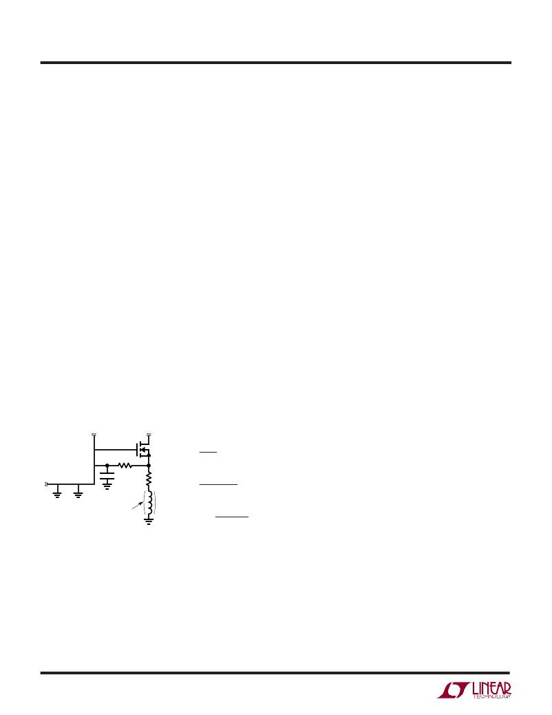
�f� =� SENSE�
�2� π� (51� ?� )C� COMP�
�R� SENSE� (51� ?� )�
�GATE�
�I� SENSE�
�SGND� PGND�
�51� ?�
�C� COMP�
�PARASITIC�
�INDUCTANCE�
�R� SENSE�
�L� P�
�1725� F05�
�SENSE� RESISTOR� ZERO� AT:�
�R�
�2� π� L� P�
�COMPENSATING� POLE� AT:�
�1�
�f=�
�FOR� CANCELLATION:�
�L� P�
�C� COMP� =�
�it� user� programmable.� As� a� rough� rule� of� thumb,� each� 4k�
�or� so� of� impedance� generates� about� 1%� of� hysteresis.�
�(This� is� based� on� roughly� 1.25V� for� the� threshold� and� 3� μ� A�
�for� the� bias� current� shift.)�
�Even� in� good� quality� ground� plane� layouts,� it� is� common�
�for� the� switching� node� (MOSFET� drain)� to� couple� to� the�
�UVLO� pin� with� a� stray� capacitance� of� several� thousandths�
�of� a� pF.� To� ensure� proper� UVLO� action,� a� 100pF� capacitor�
�Figure� 5�
�SOFT-START� FUNCTION�
�The� LT1725� contains� an� optional� soft-start� function� that� is�
�enabled� by� connecting� an� explicit� external� capacitor� be-�
�tween� the� SFST� pin� and� ground.� Internal� circuitry� prevents�
�the� control� voltage� at� the� V� C� pin� from� exceeding� that� on� the�
�is� recommended� from� this� pin� to� ground� as� shown� in�
�Figure� 6b.� This� will� typically� reduce� the� coupled� noise� to�
�a� few� millivolts.� The� UVLO� filter� capacitor� should� not� be�
�made� much� larger� than� a� few� hundred� pF,� however,� as� the�
�hysteresis� action� will� become� too� slow.� In� cases� where�
�further� filtering� is� required,� e.g.,� to� attenuate� high� speed�
�supply� ripple,� the� topology� in� Figure� 6c� is� recommended.�
�Resistor� R1� has� been� split� into� two� equal� parts.� This�
�provides� a� node� for� effecting� capacitor� filtering� of� high�
�SFST� pin.�
�1725fa�
�16�
�相关PDF资料 |
PDF描述 |
|---|---|
| UCA2V330MHD1TN | CAP ALUM 33UF 350V 20% RADIAL |
| B41042A3827M | 820UF 10V 10X20 SINGLE END |
| LT3757HMSE#TRPBF | IC REG CTRLR PWM CM 10-MSOP |
| LTC3830-1ES8#TRPBF | IC REG CTRLR BUCK PWM VM 8-SOIC |
| ADM690SQ | IC SUPERVISOR MPU 4.65V WD 8CDIP |
相关代理商/技术参数 |
参数描述 |
|---|---|
| LT1725CS | 功能描述:IC REG CTRLR FLYBK ISO CM 16SOIC RoHS:否 类别:集成电路 (IC) >> PMIC - 稳压器 - DC DC 切换控制器 系列:- 标准包装:2,500 系列:- PWM 型:电流模式 输出数:1 频率 - 最大:500kHz 占空比:96% 电源电压:4 V ~ 36 V 降压:无 升压:是 回扫:无 反相:无 倍增器:无 除法器:无 Cuk:无 隔离:无 工作温度:-40°C ~ 125°C 封装/外壳:24-WQFN 裸露焊盘 包装:带卷 (TR) |
| LT1725CS#PBF | 功能描述:IC REG CTRLR FLYBK ISO CM 16SOIC RoHS:是 类别:集成电路 (IC) >> PMIC - 稳压器 - DC DC 切换控制器 系列:- 标准包装:2,500 系列:- PWM 型:电流模式 输出数:1 频率 - 最大:500kHz 占空比:96% 电源电压:4 V ~ 36 V 降压:无 升压:是 回扫:无 反相:无 倍增器:无 除法器:无 Cuk:无 隔离:无 工作温度:-40°C ~ 125°C 封装/外壳:24-WQFN 裸露焊盘 包装:带卷 (TR) |
| LT1725CS#TR | 功能描述:IC REG CTRLR FLYBK ISO CM 16SOIC RoHS:否 类别:集成电路 (IC) >> PMIC - 稳压器 - DC DC 切换控制器 系列:- 标准包装:2,500 系列:- PWM 型:电流模式 输出数:1 频率 - 最大:500kHz 占空比:96% 电源电压:4 V ~ 36 V 降压:无 升压:是 回扫:无 反相:无 倍增器:无 除法器:无 Cuk:无 隔离:无 工作温度:-40°C ~ 125°C 封装/外壳:24-WQFN 裸露焊盘 包装:带卷 (TR) |
| LT1725CS#TRPBF | 功能描述:IC REG CTRLR FLYBK ISO CM 16SOIC RoHS:是 类别:集成电路 (IC) >> PMIC - 稳压器 - DC DC 切换控制器 系列:- 标准包装:2,500 系列:- PWM 型:电流模式 输出数:1 频率 - 最大:500kHz 占空比:96% 电源电压:4 V ~ 36 V 降压:无 升压:是 回扫:无 反相:无 倍增器:无 除法器:无 Cuk:无 隔离:无 工作温度:-40°C ~ 125°C 封装/外壳:24-WQFN 裸露焊盘 包装:带卷 (TR) |
| LT1725IGN | 功能描述:IC REG CTRLR FLYBK ISO CM 16SSOP RoHS:否 类别:集成电路 (IC) >> PMIC - 稳压器 - DC DC 切换控制器 系列:- 标准包装:2,500 系列:- PWM 型:电流模式 输出数:1 频率 - 最大:500kHz 占空比:96% 电源电压:4 V ~ 36 V 降压:无 升压:是 回扫:无 反相:无 倍增器:无 除法器:无 Cuk:无 隔离:无 工作温度:-40°C ~ 125°C 封装/外壳:24-WQFN 裸露焊盘 包装:带卷 (TR) |
发布紧急采购,3分钟左右您将得到回复。