参数资料
| 型号: | LT1762EMS8-3.3#TR |
| 厂商: | Linear Technology |
| 文件页数: | 10/16页 |
| 文件大小: | 0K |
| 描述: | IC REG LDO 3.3V .15A 8MSOP |
| 标准包装: | 2,500 |
| 稳压器拓扑结构: | 正,固定式 |
| 输出电压: | 3.3V |
| 输入电压: | 最高 20V |
| 电压 - 压降(标准): | 0.27V @ 150mA |
| 稳压器数量: | 1 |
| 电流 - 输出: | 150mA |
| 电流 - 限制(最小): | 160mA |
| 工作温度: | -40°C ~ 125°C |
| 安装类型: | 表面贴装 |
| 封装/外壳: | 8-TSSOP,8-MSOP(0.118",3.00mm 宽) |
| 供应商设备封装: | 8-MSOP |
| 包装: | 带卷 (TR) |
�� �
�
�LT1762� Series�
�PI� N� FU� N� CTIO� N� S�
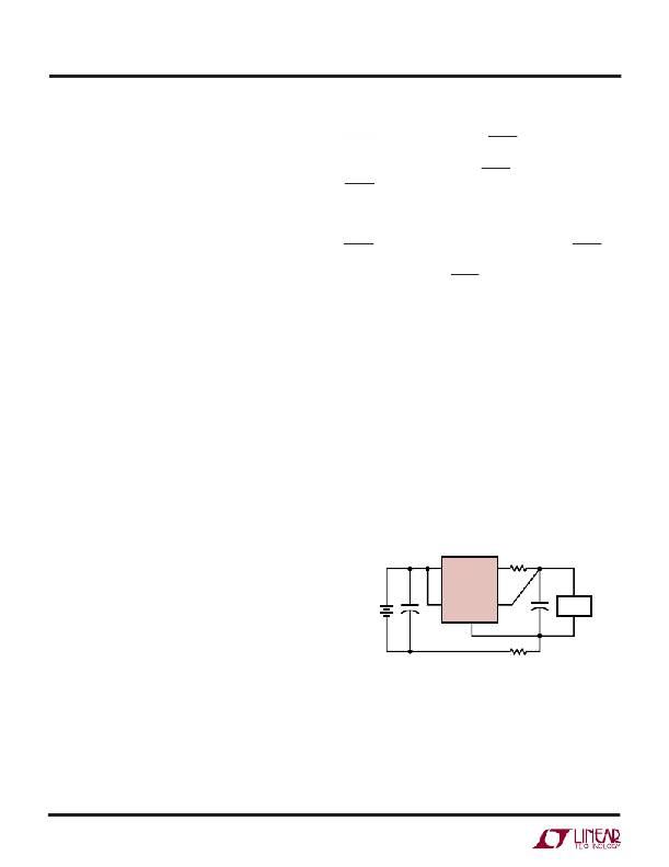
�OUT� (Pin� 1):� Output.� The� output� supplies� power� to� the�
�load.� A� minimum� output� capacitor� of� 2.2� μ� F� is� required� to�
�prevent� oscillations.� Larger� output� capacitors� will� be�
�required� for� applications� with� large� transient� loads� to� limit�
�peak� voltage� transients.� See� the� Applications� Information�
�section� for� more� information� on� output� capacitance� and�
�reverse� output� characteristics.�
�SENSE� (Pin� 2):� Output� Sense.� For� fixed� voltage� versions�
�of� the� LT1762� (LT1762-2.5/LT1762-3/LT1762-3.3/�
�LT1762-5),� the� SENSE� pin� is� the� input� to� the� error� ampli-�
�fier.� Optimum� regulation� will� be� obtained� at� the� point�
�where� the� SENSE� pin� is� connected� to� the� OUT� pin� of� the�
�regulator.� In� critical� applications,� small� voltage� drops� are�
�caused� by� the� resistance� (R� P� )� of� PC� traces� between� the�
�regulator� and� the� load.� These� may� be� eliminated� by� con-�
�necting� the� SENSE� pin� to� the� output� at� the� load� as� shown�
�in� Figure� 1� (Kelvin� Sense� Connection).� Note� that� the�
�voltage� drop� across� the� external� PC� traces� will� add� to� the�
�dropout� voltage� of� the� regulator.� The� SENSE� pin� bias�
�current� is� 10� μ� A� at� the� nominal� rated� output� voltage.� The�
�SENSE� pin� can� be� pulled� below� ground� (as� in� a� dual� supply�
�system� where� the� regulator� load� is� returned� to� a� negative�
�supply)� and� still� allow� the� device� to� start� and� operate.�
�ADJ� (Pin� 2):� Adjust.� For� the� adjustable� LT1762,� this� is� the�
�input� to� the� error� amplifier.� This� pin� is� internally� clamped�
�to� ±� 7V.� It� has� a� bias� current� of� 30nA� which� flows� into� the�
�pin� (see� curve� of� ADJ� Pin� Bias� Current� vs� Temperature� in�
�the� Typical� Performance� Characteristics).� The� ADJ� pin�
�GND� (Pin� 4):� Ground.�
�SHDN� (Pin5):� Shutdown.� The� SHDN� pin� is� used� to� put� the�
�LT1762� regulators� into� a� low� power� shutdown� state.� The�
�output� will� be� off� when� the� SHDN� pin� is� pulled� low.� The�
�SHDN� pin� can� be� driven� either� by� 5V� logic� or� open-�
�collector� logic� with� a� pull-up� resistor.� The� pull-up� resistor�
�is� required� to� supply� the� pull-up� current� of� the� open-�
�collector� gate,� normally� several� microamperes,� and� the�
�SHDN� pin� current,� typically� 1� μ� A.� If� unused,� the� SHDN� pin�
�must� be� connected� to� V� IN� .� The� device� will� be� in� low� power�
�shutdown� state� if� the� SHDN� pin� is� not� connected.�
�IN� (Pin� 8):� Input.� Power� is� supplied� to� the� device� through�
�the� IN� pin.� A� bypass� capacitor� is� required� on� this� pin� if� the�
�device� is� more� than� six� inches� away� from� the� main� input�
�filter� capacitor.� In� general,� the� output� impedance� of� a�
�battery� rises� with� frequency,� so� it� is� advisable� to� include� a�
�bypass� capacitor� in� battery-powered� circuits.� A� bypass�
�capacitor� in� the� range� of� 1� μ� F� to� 10� μ� F� is� sufficient.� The�
�LT1762� regulators� are� designed� to� withstand� reverse�
�voltages� on� the� IN� pin� with� respect� to� ground� and� the� OUT�
�pin.� In� the� case� of� a� reverse� input,� which� can� happen� if� a�
�battery� is� plugged� in� backwards,� the� device� will� act� as� if�
�there� is� a� diode� in� series� with� its� input.� There� will� be� no�
�reverse� current� flow� into� the� regulator� and� no� reverse�
�voltage� will� appear� at� the� load.� The� device� will� protect� both�
�itself� and� the� load.�
�voltage� is� 1.22V� referenced� to� ground� and� the� output�
�8�
�IN�
�OUT�
�1�
�R� P�
�voltage� range� is� 1.22V� to� 20V.�
�BYP� (Pins� 3):� Bypass.� The� BYP� pin� is� used� to� bypass� the�
�reference� of� the� LT1762� regulators� to� achieve� low� noise�
�V� IN�
�+�
�5�
�LT1762�
�SHDN� SENSE�
�GND�
�2�
�+�
�LOAD�
�performance� from� the� regulator.� The� BYP� pin� is� clamped�
�internally� to� ±� 0.6V� (one� V� BE� ).� A� small� capacitor� from� the�
�4�
�R� P�
�1762� F01�
�output� to� this� pin� will� bypass� the� reference� to� lower� the�
�output� voltage� noise.� A� maximum� value� of� 0.01� μ� F� can� be�
�used� for� reducing� output� voltage� noise� to� a� typical� 20� μ� V� RMS�
�Figure� 1.� Kelvin� Sense� Connection�
�over� a� 10Hz� to� 100kHz� bandwidth.� If� not� used,� this� pin�
�must� be� left� unconnected.�
�1762fa�
�10�
�相关PDF资料 |
PDF描述 |
|---|---|
| LT1763MPDE-2.5#PBF | IC REG LDO 2.5V .5A 12-DFN |
| LT1764AMPQ#TRPBF | IC REG LDO ADJ 3A DDPAK-5 |
| LT1765EFE-1.8 | IC REG BUCK 1.8V 3A 16TSSOP |
| LT1766HFE#TRPBF | IC REG BUCK ADJ 1.5A 16TSSOP |
| LT1767EMS8-2.5 | IC REG BUCK 2.5V 1.5A 8MSOP |
相关代理商/技术参数 |
参数描述 |
|---|---|
| LT1762EMS8-5 | 功能描述:IC REG LDO 5V .15A 8MSOP RoHS:否 类别:集成电路 (IC) >> PMIC - 稳压器 - 线性 系列:- 标准包装:1 系列:- 稳压器拓扑结构:正,固定式 输出电压:3.3V 输入电压:2.5 V ~ 5.5 V 电压 - 压降(标准):0.1V @ 200mA 稳压器数量:2 电流 - 输出:300mA 电流 - 限制(最小):350mA 工作温度:-40°C ~ 85°C 安装类型:表面贴装 封装/外壳:8-UFQFN 供应商设备封装:8-MLPQ-UT(1.5x1.5) 包装:剪切带 (CT) 产品目录页面:1358 (CN2011-ZH PDF) 其它名称:SC560HULCT |
| LT1762EMS8-5#PBF | 功能描述:IC REG LDO 5V .15A 8MSOP RoHS:是 类别:集成电路 (IC) >> PMIC - 稳压器 - 线性 系列:- 产品培训模块:MIC5365/66 Ultra-small LDO Regulators 标准包装:1 系列:- 稳压器拓扑结构:正,固定式 输出电压:3V 输入电压:最高 5.5V 电压 - 压降(标准):0.155V @ 150mA 稳压器数量:1 电流 - 输出:150mA 电流 - 限制(最小):200mA 工作温度:-40°C ~ 125°C 安装类型:表面贴装 封装/外壳:4-UDFN 裸露焊盘,4-TMLF? 供应商设备封装:4-TMLF?(1x1) 包装:Digi-Reel® 其它名称:576-3192-6 |
| LT1762EMS8-5#TR | 功能描述:IC REG LDO 5V .15A 8MSOP RoHS:否 类别:集成电路 (IC) >> PMIC - 稳压器 - 线性 系列:- 标准包装:1 系列:- 稳压器拓扑结构:正,固定式 输出电压:3.3V 输入电压:2.5 V ~ 5.5 V 电压 - 压降(标准):0.1V @ 200mA 稳压器数量:2 电流 - 输出:300mA 电流 - 限制(最小):350mA 工作温度:-40°C ~ 85°C 安装类型:表面贴装 封装/外壳:8-UFQFN 供应商设备封装:8-MLPQ-UT(1.5x1.5) 包装:剪切带 (CT) 产品目录页面:1358 (CN2011-ZH PDF) 其它名称:SC560HULCT |
| LT1762EMS8-5#TRPBF | 功能描述:IC REG LDO 5V .15A 8MSOP RoHS:是 类别:集成电路 (IC) >> PMIC - 稳压器 - 线性 系列:- 标准包装:1 系列:- 稳压器拓扑结构:正,固定式 输出电压:3.3V 输入电压:2.5 V ~ 5.5 V 电压 - 压降(标准):0.1V @ 200mA 稳压器数量:2 电流 - 输出:300mA 电流 - 限制(最小):350mA 工作温度:-40°C ~ 85°C 安装类型:表面贴装 封装/外壳:8-UFQFN 供应商设备封装:8-MLPQ-UT(1.5x1.5) 包装:剪切带 (CT) 产品目录页面:1358 (CN2011-ZH PDF) 其它名称:SC560HULCT |
| LT1762EMS8-5PBF | 制造商:Linear Technology 功能描述:LDO Regulator 5V 150mA Low Noise MSOP8 |
发布紧急采购,3分钟左右您将得到回复。