- 您现在的位置:买卖IC网 > PDF目录14048 > LT1767EMS8-1.8#TRPBF (Linear Technology)IC REG BUCK 1.8V 1.5A 8MSOP PDF资料下载
参数资料
| 型号: | LT1767EMS8-1.8#TRPBF |
| 厂商: | Linear Technology |
| 文件页数: | 11/16页 |
| 文件大小: | 0K |
| 描述: | IC REG BUCK 1.8V 1.5A 8MSOP |
| 标准包装: | 2,500 |
| 类型: | 降压(降压) |
| 输出类型: | 固定 |
| 输出数: | 1 |
| 输出电压: | 1.8V |
| 输入电压: | 3 V ~ 25 V |
| PWM 型: | 电流模式 |
| 频率 - 开关: | 1.25MHz |
| 电流 - 输出: | 1.5A |
| 同步整流器: | 无 |
| 工作温度: | -40°C ~ 125°C |
| 安装类型: | 表面贴装 |
| 封装/外壳: | 8-TSSOP,8-MSOP(0.118",3.00mm 宽) |
| 包装: | 带卷 (TR) |
| 供应商设备封装: | 8-MSOP |
�� �
�
�LT1767/LT1767-1.8/�
�LT1767-2.5/LT1767-3.3/LT1767-5�
�APPLICATIO� N� S� I� N� FOR� M� ATIO� N�
�prevent� subharmonic� switching� is� reduced.� This� type� of�
�subharmonic� switching� only� occurs� at� input� voltages� less�
�than� twice� output� voltage.� Higher� inductor� values� will� tend�
�to� eliminate� this� problem.� See� Frequency� Compensation�
�section� for� a� discussion� of� an� entirely� different� cause� of�
�subharmonic� switching� before� assuming� that� the� cause� is�
�insufficient� slope� compensation.� Application� Note� 19� has�
�more� details� on� the� theory� of� slope� compensation.�
�LAYOUT� CONSIDERATIONS�
�As� with� all� high� frequency� switchers,� when� considering�
�layout,� care� must� be� taken� in� order� to� achieve� optimal�
�electrical,� thermal� and� noise� performance.� For� maximum�
�efficiency,� switch� rise� and� fall� times� are� typically� in� the�
�nanosecond� range.� To� prevent� noise� both� radiated� and�
�conducted,� the� high� speed� switching� current� path,� shown�
�in� Figure� 5,� must� be� kept� as� short� as� possible.� This� is�
�implemented� in� the� suggested� layout� of� Figure� 6.� Shorten-�
�Board� layout� also� has� a� significant� effect� on� thermal�
�resistance.� Soldering� the� exposed� pad� to� as� large� a� copper�
�area� as� possible� and� placing� feedthroughs� under� the� pad�
�to� a� ground� plane,� will� reduce� die� temperature� and� in-�
�crease� the� power� capacity� of� the� LT1767.� For� the�
�nonexposed� package,� Pin� 4� is� connected� directly� to� the�
�pad� inside� the� package.� Similar� treatment� of� this� pin� will�
�result� in� lower� die� temperatures.�
�THERMAL� CALCULATIONS�
�Power� dissipation� in� the� LT1767� chip� comes� from� four�
�sources:� switch� DC� loss,� switch� AC� loss,� boost� circuit�
�current,� and� input� quiescent� current.� The� following�
�formulas� show� how� to� calculate� each� of� these� losses.�
�These� formulas� assume� continuous� mode� operation,� so�
�they� should� not� be� used� for� calculating� efficiency� at� light�
�load� currents.�
�Switch� loss:�
�(� )� (� V� OUT� )� +� 17� ns� (� I� OUT� )(� V� IN� )(� )� f�
�ingthispathwillalsoreducetheparasitictraceinductance�
�of� approximately� 25nH/inch.� At� switch� off,� this� parasitic�
�inductance� produces� a� flyback� spike� across� the� LT1767�
�switch.� When� operating� at� higher� currents� and� input�
�P� SW� =�
�2�
�R� SW� I� OUT�
�V� IN�
�voltages,� with� poor� layout,� this� spike� can� generate� volt-�
�Boost� current� loss� for� V� BOOST� =� V� OUT� :�
�(� )�
�ages across the LT1767 that may exceed its absolute�
�maximum� rating.� A� ground� plane� should� always� be� used�
�under� the� switcher� circuitry� to� prevent� interplane� coupling�
�and� overall� noise.�
�P� BOOST� =�
�2�
�V� OUT� I� OUT� /� 50�
�V� IN�
�Quiescent� current� loss:�
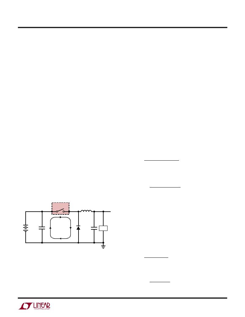
�V� IN�
�LT1767�
�SW�
�L1�
�5V�
�P� Q� =� V� IN� (� 0� .� 001� )�
�HIGH�
�R� SW� =� Switch� resistance� (� ≈� 0.27� ?� when� hot)�
�V� IN� C3�
�FREQUENCY�
�CIRCULATING�
�PATH�
�D1� C1�
�LOAD�
�17ns� =� Equivalent� switch� current/voltage� overlap� time�
�f� =� Switch� frequency�
�Example:� with� V� IN� =� 10V,� V� OUT� =� 5V� and� I� OUT� =� 1A:�
�(� )(� )� (� )� 5� +� 17� ?� 10� (� )(� )� 1� .� 25� ?� 10� 6�
�(�
�)�
�(�
�)�
�?� 9� 1� 10�
�(� 5� )� (� 1� /� 50� )� =� 0� .� 05� W�
�(�
�)�
�1767� F05�
�Figure� 5.� High� Speed� Switching� Path�
�The� V� C� and� FB� components� should� be� kept� as� far� away� as�
�possible� from� the� switch� and� boost� nodes.� The� LT1767�
�pinout� has� been� designed� to� aid� in� this.� The� ground� for�
�these� components� should� be� separated� from� the� switch�
�current� path.� Failure� to� do� so� will� result� in� poor� stability� or�
�subharmonic� like� oscillation.�
�2�
�0� .� 27� 1�
�P� SW� =�
�10�
�=� 0� .� 135� +� 0� .� 21� =� 0� .� 34� W�
�2�
�P� BOOST� =�
�10�
�P� Q� =� 10� 0� .� 001� =� 0� .� 01� W�
�sn1767� 1767fas�
�11�
�相关PDF资料 |
PDF描述 |
|---|---|
| MAX6868UK46D3S+T | IC MPU SUPERVISOR SOT23-5 |
| 50MH70.47MEFCT54X7 | CAP ALUM 0.47UF 50V 20% RADIAL |
| MAX6868UK45D4L+T | IC MPU SUPERVISOR SOT23-5 |
| LT1767EMS8-5#TRPBF | IC REG BUCK 5V 1.5A 8MSOP |
| 50MH70.47MEFCTZ4X7 | CAP ALUM 0.47UF 50V 20% RADIAL |
相关代理商/技术参数 |
参数描述 |
|---|---|
| LT1767EMS8-2.5 | 功能描述:IC REG BUCK 2.5V 1.5A 8MSOP RoHS:否 类别:集成电路 (IC) >> PMIC - 稳压器 - DC DC 开关稳压器 系列:- 设计资源:Design Support Tool 标准包装:1 系列:- 类型:升压(升压) 输出类型:固定 输出数:1 输出电压:3V 输入电压:0.75 V ~ 2 V PWM 型:- 频率 - 开关:- 电流 - 输出:100mA 同步整流器:是 工作温度:-40°C ~ 85°C 安装类型:表面贴装 封装/外壳:SOT-23-5 细型,TSOT-23-5 包装:剪切带 (CT) 供应商设备封装:TSOT-23-5 其它名称:AS1323-BTTT-30CT |
| LT1767EMS8-2.5#PBF | 功能描述:IC REG BUCK 2.5V 1.5A 8MSOP RoHS:是 类别:集成电路 (IC) >> PMIC - 稳压器 - DC DC 开关稳压器 系列:- 标准包装:250 系列:- 类型:降压(降压) 输出类型:固定 输出数:1 输出电压:1.2V 输入电压:2.05 V ~ 6 V PWM 型:电压模式 频率 - 开关:2MHz 电流 - 输出:500mA 同步整流器:是 工作温度:-40°C ~ 85°C 安装类型:表面贴装 封装/外壳:6-UFDFN 包装:带卷 (TR) 供应商设备封装:6-SON(1.45x1) 产品目录页面:1032 (CN2011-ZH PDF) 其它名称:296-25628-2 |
| LT1767EMS8-2.5#TR | 功能描述:IC REG BUCK 2.5V 1.5A 8MSOP RoHS:否 类别:集成电路 (IC) >> PMIC - 稳压器 - DC DC 开关稳压器 系列:- 标准包装:2,500 系列:- 类型:降压(降压) 输出类型:固定 输出数:1 输出电压:1.2V,1.5V,1.8V,2.5V 输入电压:2.7 V ~ 20 V PWM 型:- 频率 - 开关:- 电流 - 输出:50mA 同步整流器:是 工作温度:-40°C ~ 125°C 安装类型:表面贴装 封装/外壳:10-TFSOP,10-MSOP(0.118",3.00mm 宽)裸露焊盘 包装:带卷 (TR) 供应商设备封装:10-MSOP 裸露焊盘 |
| LT1767EMS8-2.5#TRPBF | 功能描述:IC REG BUCK 2.5V 1.5A 8MSOP RoHS:是 类别:集成电路 (IC) >> PMIC - 稳压器 - DC DC 开关稳压器 系列:- 标准包装:2,500 系列:- 类型:降压(降压) 输出类型:固定 输出数:1 输出电压:1.2V,1.5V,1.8V,2.5V 输入电压:2.7 V ~ 20 V PWM 型:- 频率 - 开关:- 电流 - 输出:50mA 同步整流器:是 工作温度:-40°C ~ 125°C 安装类型:表面贴装 封装/外壳:10-TFSOP,10-MSOP(0.118",3.00mm 宽)裸露焊盘 包装:带卷 (TR) 供应商设备封装:10-MSOP 裸露焊盘 |
| LT1767EMS8-3.3 | 功能描述:IC REG BUCK 3.3V 1.5A 8MSOP RoHS:否 类别:集成电路 (IC) >> PMIC - 稳压器 - DC DC 开关稳压器 系列:- 标准包装:2,500 系列:- 类型:降压(降压) 输出类型:固定 输出数:1 输出电压:1.2V,1.5V,1.8V,2.5V 输入电压:2.7 V ~ 20 V PWM 型:- 频率 - 开关:- 电流 - 输出:50mA 同步整流器:是 工作温度:-40°C ~ 125°C 安装类型:表面贴装 封装/外壳:10-TFSOP,10-MSOP(0.118",3.00mm 宽)裸露焊盘 包装:带卷 (TR) 供应商设备封装:10-MSOP 裸露焊盘 |
发布紧急采购,3分钟左右您将得到回复。