- 您现在的位置:买卖IC网 > PDF目录2155 > LT1886CS8#TRPBF (Linear Technology)IC OPAMP DUAL 200MA 700MHZ 8SOIC PDF资料下载
参数资料
| 型号: | LT1886CS8#TRPBF |
| 厂商: | Linear Technology |
| 文件页数: | 3/16页 |
| 文件大小: | 0K |
| 描述: | IC OPAMP DUAL 200MA 700MHZ 8SOIC |
| 标准包装: | 2,500 |
| 放大器类型: | 通用 |
| 电路数: | 2 |
| 转换速率: | 200 V/µs |
| 增益带宽积: | 700MHz |
| 电流 - 输入偏压: | 1.5µA |
| 电压 - 输入偏移: | 1000µV |
| 电流 - 电源: | 7mA |
| 电流 - 输出 / 通道: | 800mA |
| 电压 - 电源,单路/双路(±): | 4 V ~ 13 V,±2 V ~ 6.5 V |
| 工作温度: | 0°C ~ 70°C |
| 安装类型: | 表面贴装 |
| 封装/外壳: | 8-SOIC(0.154",3.90mm 宽) |
| 供应商设备封装: | 8-SO |
| 包装: | 带卷 (TR) |
11
LT1886
APPLICATIO S I FOR ATIO
WU
U
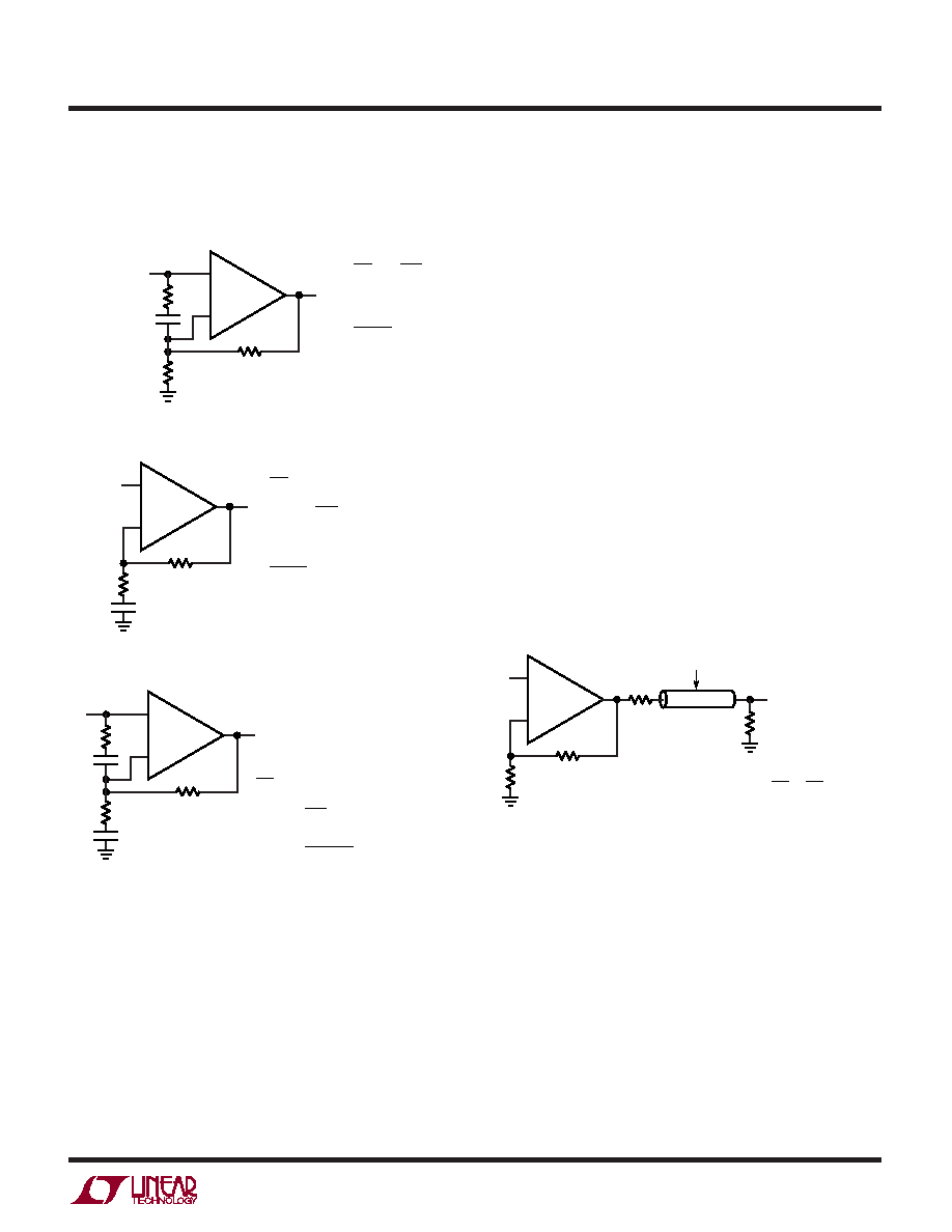
Figures 3 and 4 can be combined as shown in Figure 5. The
gain is unity at low frequencies, 1 + RF/RG at mid-band and
for stability, a gain of 10 or greater at high frequencies.
termination resistor is used, a capacitor to ground at the
load can eliminate ringing.
Line Driving Back-Termination
The standard method of cable or line back-termination is
shown in Figure 6. The cable/line is terminated in its
characteristic impedance (50
, 75, 100, 135, etc.).
A back-termination resistor also equal to to the
chararacteristic impedance should be used for maximum
pulse fidelity of outgoing signals, and to terminate the line
for incoming signals in a full-duplex application. There are
three main drawbacks to this approach. First, the power
dissipated in the load and back-termination resistors is
equal so half of the power delivered by the amplifier is
wasted in the termination resistor. Second, the signal is
halved so the gain of the amplifer must be doubled to have
the same overall gain to the load. The increase in gain
increases noise and decreases bandwidth (which can also
increase distortion). Third, the output swing of the ampli-
fier is doubled which can limit the power it can deliver to
the load for a given power supply voltage.
RC
Vo
Vi
CC
(OPTIONAL)
+
–
1886 F03
RF
RG
= 1 +
RF
RG
Vo
Vi
< 15MHz
1
2
πRCCC
(RC || RG) ≤ RF/9
Output Loading
The LT1886 output stage is very wide bandwidth and able
to source and sink large currents. Reactive loading, even
isolated with a back-termination resistor, can cause ring-
ing at frequencies of hundreds of MHz. For this reason, any
design should be evaluated over a wide range of output
conditions. To reduce the effects of reactive loading, an
optional snubber network consisting of a series RC across
the load can provide a resistive load at high frequency.
Another option is to filter the drive to the load. If a back-
Figure 3. Compensation for Noninverting Gains
+
–
1886 F04
RF
RG
Vi
VO
CC
< 15MHz
1
2
πRGCC
RG ≤ RF/9
= 1 (LOW FREQUENCIES)
(HIGH FREQUENCIES)
Vo
Vi
= 1 +
RF
RG
Figure 4. Alternate Noninverting Compensation
RC
Vo
Vi
CC
+
–
1886 F05
RF
RG
CBIG
RF
RG
= 1 AT LOW FREQUENCIES
= 1 +
AT MEDIUM FREQUENCIES
RF
(RC || RG)
= 1 +
AT HIGH FREQUENCIES
Vo
Vi
Figure 5. Combination Compensation
+
–
1886 F06
RF
RBT
CABLE OR LINE WITH
CHARACTERISTIC IMPEDANCE RL
RG
VO
Vi
RL
(1 + RF/RG)
=
Vo
Vi
1
2
RBT = RL
An alternate method of back-termination is shown in
Figure 7. Positive feedback increases the effective back-
termination resistance so RBT can be reduced by a factor
of n. To analyze this circuit, first ground the input. As RBT =
RL/n, and assuming RP2>>RL we require that:
Va = Vo (1 – 1/n) to increase the effective value of
RBT by n.
Vp = Vo (1 – 1/n)/(1 + RF/RG)
Vo = Vp (1 + RP2/RP1)
Eliminating Vp, we get the following:
(1 + RP2/RP1) = (1 + RF/RG)/(1 – 1/n)
Figure 6. Standard Cable/Line Back-Termination
相关PDF资料 |
PDF描述 |
|---|---|
| LT1920IS8#TRPBF | IC AMP INSTRUMENT PREC LP 8SOIC |
| LT1969CMS#TRPBF | IC OP-AMP ADJ CURRNT DUAL 10MSOP |
| LT1970IFE#TRPBF | IC OP AMP 500MA ADJ 20-TSSOP |
| LT1990AHS8#TRPBF | IC AMP DIFF +/-250V MCRPWR 8SOIC |
| LT1993CUD-10#TRPBF | IC DIFF AMP/ADC DRVR 16-QFN |
相关代理商/技术参数 |
参数描述 |
|---|---|
| LT1893-11-0125 | 制造商:未知厂家 制造商全称:未知厂家 功能描述:PHOTOTRANSISTOR | NPN | DOME-5.0 |
| LT18E-Q21-LU0X3-H1141 | 制造商:TURCK Inc 功能描述:LT0102 |
| LT190 | 制造商:Cooper Wiring Devices 功能描述: |
| LT190Z | 制造商:SEOUL 制造商全称:Seoul Semiconductor 功能描述:GREEN OVAL LAMP LED |
| LT191 | 制造商:SEOUL 制造商全称:Seoul Semiconductor 功能描述:BLUE OVAL LAMP LED |
发布紧急采购,3分钟左右您将得到回复。