- 您现在的位置:买卖IC网 > PDF目录15300 > LT1952IGN#TRPBF (Linear Technology)IC REG CTRLR ISO PWM CM 16-SSOP PDF资料下载
参数资料
| 型号: | LT1952IGN#TRPBF |
| 厂商: | Linear Technology |
| 文件页数: | 16/28页 |
| 文件大小: | 0K |
| 描述: | IC REG CTRLR ISO PWM CM 16-SSOP |
| 标准包装: | 2,500 |
| PWM 型: | 电流模式 |
| 输出数: | 1 |
| 频率 - 最大: | 560kHz |
| 占空比: | 90% |
| 电源电压: | 9.25 V ~ 25 V |
| 降压: | 无 |
| 升压: | 无 |
| 回扫: | 无 |
| 反相: | 无 |
| 倍增器: | 无 |
| 除法器: | 无 |
| Cuk: | 无 |
| 隔离: | 是 |
| 工作温度: | -40°C ~ 125°C |
| 封装/外壳: | 16-SSOP(0.154",3.90mm 宽) |
| 包装: | 带卷 (TR) |
第1页第2页第3页第4页第5页第6页第7页第8页第9页第10页第11页第12页第13页第14页第15页当前第16页第17页第18页第19页第20页第21页第22页第23页第24页第25页第26页第27页第28页
�� �
�
�LT1952/LT1952-1�
�APPLICATIONS� INFORMATION�
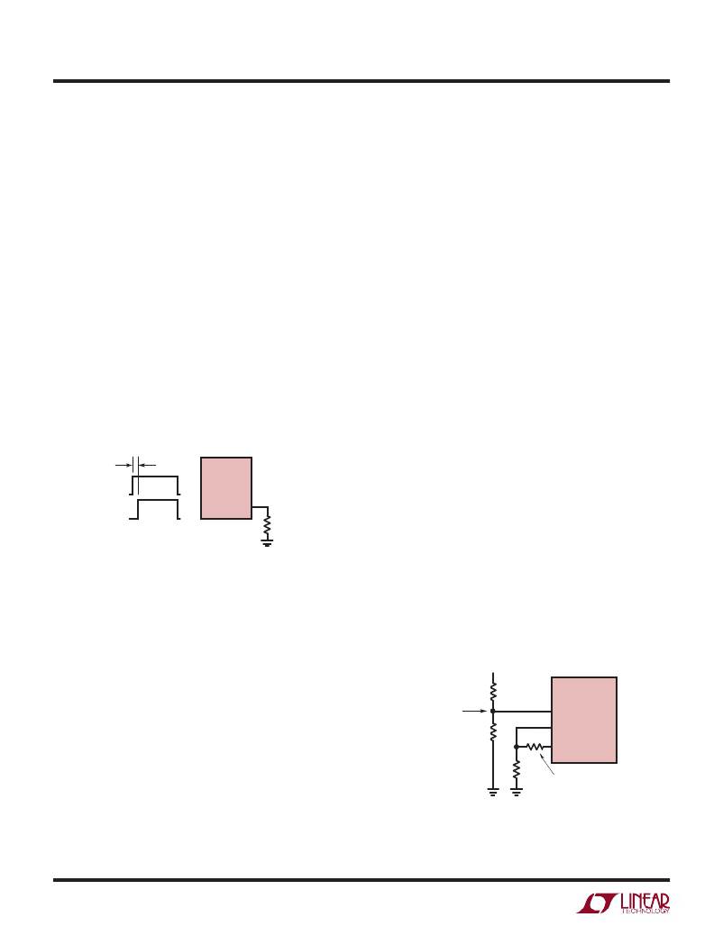
�Programming� Synchronous� Rectifier� Timing:�
�SOUT� to� OUT� delay� (‘t� DELAY� ’)�
�The� LT1952/LT1952-1� have� an� additional� output� SOUT�
�which� provides� a� ±� 50mA� peak� drive� clamped� to� 12V.� In�
�applications� requiring� synchronous� rectification� for� high�
�efficiency,� the� LT1952/LT1952-1� SOUT� provides� a� sync�
�signal� for� secondary� side� control� of� the� synchronous�
�rectifier� MOSFETs� (Figure� 11).� Timing� delays� through� the�
�converter� can� cause� non-optimum� control� timing� for� the�
�synchronous� rectifier� MOSFETs.� The� LT1952/LT1952-1�
�provide� a� programmable� delay� (t� DELAY� ,� Figure� 8)� between�
�SOUT� rising� edge� and� OUT� rising� edge� to� optimize� timing�
�control� for� the� synchronous� rectifier� MOSFETs� to� achieve�
�maximum� efficiency� gains.� A� resistor� R� DELAY� connected�
�from� the� DELAY� pin� to� ground� sets� the� value� of� t� DELAY� .�
�Typical� values� for� t� DELAY� range� from� 10ns� with� R� DELAY� =�
�10k� to� 160ns� with� R� DELAY� =� 160k.� (see� graph� in� Typical�
�Performance� Characteristics)�
�SS_MAXDC� pin� using� a� resistor� divider� from� V� REF� .� An�
�increase� of� voltage� at� the� SS_MAXDC� pin� causes� the�
�maximum� duty� cycle� clamp� to� increase.�
�To� program� the� volt-second� clamp,� the� following� steps�
�should� be� taken:�
�(1)The� maximum� operational� duty� cycle� of� the� converter�
�should� be� calculated� for� the� given� application.�
�(2)An� initial� value� for� the� maximum� duty� cycle� clamp�
�should� be� calculated� using� the� equation� below� with� a�
�first� pass� guess� for� SS_MAXDC.�
�Note:� Since� maximum� operational� duty� cycle� occurs� at�
�minimum� system� input� voltage� (UVLO),� the� voltage� at� the�
�SD_V� SEC� pin� =� 1.32V.�
�Max� Duty� Cycle� Clamp� (OUT� pin)�
� � = k ? 0.522(SS_MAXDC(DC)/SD_V� SEC� )� –�
�(t� DELAY� ? f� OSC� )�
�SOUT�
�t� DELAY�
�LT1952/�
�LT1952-1�
�where,�
�SS_MAXDC(DC)� =� V� REF� (R� B� /(R� T� +� R� B� )�
�SD_V� SEC� =� 1.32V� at� minimum� system� input� voltage�
�OUT�
�DELAY�
�1952� F08�
�R� DELAY�
�t� DELAY� =� programmed� delay� between� SOUT� and� OUT�
�k� =� 1.11� –� 5.5e� –7� ? (f� OSC� )�
�LT1952-1�
�R2�
�R� B�
�Figure8.ProgrammingSOUTtoOUTDelay:t� DELAY�
�Programming� Maximum� Duty� Cycle� Clamp�
�For� forward� converter� applications� using� the� simplest�
�topology� of� a� single� MOSFET� on� the� primary,� a� maximum�
�switch� duty� cycle� clamp� which� adapts� to� transformer�
�input� voltage� is� necessary� for� reliable� control� of� the�
�MOSFET.� This� volt-second� clamp� provides� a� safeguard� for�
�transformer� reset� that� prevents� transformer� saturation.� The�
�LT1952/LT1952-1� SD_V� SEC� and� SS_MAXDC� pins� provide� a�
�capacitor-less,� programmable� volt-second� clamp� solution�
�using� simple� resistor� ratios� (Figure� 9).�
�An� increase� of� voltage� at� the� SD_V� SEC� pin� causes� the�
�maximum� duty� cycle� clamp� to� decrease.� Deriving� SD_V� SEC�
�from� a� resistor� divider� connected� to� system� input� voltage�
�creates� the� volt-second� clamp.� The� maximum� duty� cycle�
�clamp� can� be� adjusted� by� programming� voltage� on� the�
�(3)� The� maximum� duty� cycle� clamp� calculated� in� (2)� should�
�be� programmed� to� be� 10%� greater� than� the� maximum�
�operational� duty� cycle� calculated� in� (1).� Simple� adjust-�
�ment� of� maximum� duty� cycle� can� be� achieved� by� adjusting�
�SS_MAXDC.�
�SYSTEM�
�INPUT� VOLTAGE�
�LT1952/�
�R1�
�ADAPTIVE�
�DUTY� CYCLE� SD_V� SEC�
�CLAMP� INPUT�
�SS_MAXDC�
�R� T� *�
�V� REF�
�1952� F09�
�MAX� DUTY� CYCLE�
�CLAMP� ADJUST� INPUT�
�*MINIMUM� ALLOWABLE� R� T� IS� 10k� TO�
�GUARANTEE� SOFT-START� PULL-OFF�
�Figure� 9.� Programming� Maximum� Duty� Cycle� Clamp�
�19521fe�
�16�
�相关PDF资料 |
PDF描述 |
|---|---|
| SLP153M010A5P3 | CAP ALUM 15000UF 10V 20% SNAP |
| VE-25L-EW-F3 | CONVERTER MOD DC/DC 28V 100W |
| SLP103M016C1P3 | CAP ALUM 10000UF 16V 20% SNAP |
| AS1901-C31-T | IC SUPERVISOR ACT LOW SOT23-3 |
| IMC1210EB47NJ | INDUCTOR WW 47NH 5% 1210 |
相关代理商/技术参数 |
参数描述 |
|---|---|
| LT1952MPGN#PBF | 功能描述:IC REG CTRLR ISO PWM CM 16-SSOP RoHS:是 类别:集成电路 (IC) >> PMIC - 稳压器 - DC DC 切换控制器 系列:- 标准包装:4,500 系列:PowerWise® PWM 型:控制器 输出数:1 频率 - 最大:1MHz 占空比:95% 电源电压:2.8 V ~ 5.5 V 降压:是 升压:无 回扫:无 反相:无 倍增器:无 除法器:无 Cuk:无 隔离:无 工作温度:-40°C ~ 125°C 封装/外壳:6-WDFN 裸露焊盘 包装:带卷 (TR) 配用:LM1771EVAL-ND - BOARD EVALUATION LM1771 其它名称:LM1771SSDX |
| LT1952MPGN#TRPBF | 功能描述:IC REG CTRLR ISO PWM CM 16-SSOP RoHS:是 类别:集成电路 (IC) >> PMIC - 稳压器 - DC DC 切换控制器 系列:- 标准包装:4,500 系列:PowerWise® PWM 型:控制器 输出数:1 频率 - 最大:1MHz 占空比:95% 电源电压:2.8 V ~ 5.5 V 降压:是 升压:无 回扫:无 反相:无 倍增器:无 除法器:无 Cuk:无 隔离:无 工作温度:-40°C ~ 125°C 封装/外壳:6-WDFN 裸露焊盘 包装:带卷 (TR) 配用:LM1771EVAL-ND - BOARD EVALUATION LM1771 其它名称:LM1771SSDX |
| LT1952MPGN-1#PBF | 功能描述:IC REG CTRLR ISO PWM CM 16-SSOP RoHS:是 类别:集成电路 (IC) >> PMIC - 稳压器 - DC DC 切换控制器 系列:- 标准包装:4,500 系列:PowerWise® PWM 型:控制器 输出数:1 频率 - 最大:1MHz 占空比:95% 电源电压:2.8 V ~ 5.5 V 降压:是 升压:无 回扫:无 反相:无 倍增器:无 除法器:无 Cuk:无 隔离:无 工作温度:-40°C ~ 125°C 封装/外壳:6-WDFN 裸露焊盘 包装:带卷 (TR) 配用:LM1771EVAL-ND - BOARD EVALUATION LM1771 其它名称:LM1771SSDX |
| LT1952MPGN-1#TRPBF | 功能描述:IC REG CTRLR ISO PWM CM 16-SSOP RoHS:是 类别:集成电路 (IC) >> PMIC - 稳压器 - DC DC 切换控制器 系列:- 标准包装:4,500 系列:PowerWise® PWM 型:控制器 输出数:1 频率 - 最大:1MHz 占空比:95% 电源电压:2.8 V ~ 5.5 V 降压:是 升压:无 回扫:无 反相:无 倍增器:无 除法器:无 Cuk:无 隔离:无 工作温度:-40°C ~ 125°C 封装/外壳:6-WDFN 裸露焊盘 包装:带卷 (TR) 配用:LM1771EVAL-ND - BOARD EVALUATION LM1771 其它名称:LM1771SSDX |
| LT1956 | 制造商:LINEAR 制造商全称:LINEAR 功能描述:100V Synchronous Switching Regulator Controller |
发布紧急采购,3分钟左右您将得到回复。