- 您现在的位置:买卖IC网 > PDF目录13833 > LT3434IFE (Linear Technology)IC REG BUCK ADJ 3A 16TSSOP PDF资料下载
参数资料
| 型号: | LT3434IFE |
| 厂商: | Linear Technology |
| 文件页数: | 18/24页 |
| 文件大小: | 0K |
| 描述: | IC REG BUCK ADJ 3A 16TSSOP |
| 标准包装: | 95 |
| 类型: | 降压(降压) |
| 输出类型: | 可调式 |
| 输出数: | 1 |
| 输出电压: | 1.25 V ~ 54 V |
| 输入电压: | 3.3 V ~ 60 V |
| PWM 型: | 电流模式,混合 |
| 频率 - 开关: | 200kHz |
| 电流 - 输出: | 3A |
| 同步整流器: | 无 |
| 工作温度: | -40°C ~ 125°C |
| 安装类型: | 表面贴装 |
| 封装/外壳: | 16-TSSOP(0.173",4.40mm)裸露焊盘 |
| 包装: | 管件 |
| 供应商设备封装: | 16-TSSOP-EP |
�� �
�
�LT3434�
�APPLICATIO� S� I� FOR� ATIO�
�=� 1� .� 3� M� ?�
�R� 1� =�
�5� (� 1� .� 3� M� ?� )�
�–� 1� μ� A� –�
�Example:�
�12� –� 2�
�1� .� 5� (� 5� μ� A� )�
�R� 3� =� =� 6� .� 5� M� ?� (Nearest� 1%� 6.49M� ?� )�
�1�
�1.3�
�R2� =�
�7� –� 1.3� 1� .� 3�
�1.3M� ?� 6� .� 49� M� ?�
�=� 408� k� (Nearest� 1%� 412k)�
�See� the� Typical� Performance� Characteristics� section� for�
�graphs� of� SHDN� and� V� IN� currents� verses� input� voltage.�
�Frequency� Compensation� section� for� a� discussion� of� an�
�entirely� different� cause� of� subharmonic� switching� before�
�assuming� that� the� cause� is� insufficient� slope� compensa-�
�tion.� Application� Note� 19� has� more� details� on� the� theory�
�of� slope� compensation.�
�If� the� FB� pin� voltage� is� below� 0.9V� (power-up� or� output�
�short-circuit� conditions)� the� sync� function� is� disabled.�
�This� allows� the� frequency� foldback� to� operate� to� avoid� and�
�hazardous� conditions� for� the� SW� pin.�
�If� the� synchronization� signal� is� present� during� Burst� Mode�
�operation,� synchronization� will� occur� during� the� burst�
�portion� of� the� output� waveform.� Synchronizing� the� LT3434�
�during� Burst� Mode� operation� may� alter� the� natural� burst�
�frequency� which� can� lead� to� jitter� and� increased� ripple� in�
�the� burst� waveform.�
�LT3434�
�4�
�V� IN�
�+�
�V� IN�
�If� no� synchronization� is� required� this� pin� should� be� con-�
�nected� to� ground.�
�COMP�
�V� OUT�
�R3�
�R1�
�R2�
�15�
�SHDN�
�3� μ� A�
�2.4V�
�1.3V�
�–�
�+�
�SHDN�
�COMP�
�–�
�ENABLE�
�POWER� GOOD�
�The� LT3434� contains� a� power� good� block� which� consists�
�of� a� comparator,� delay� timer� and� active� low� flag� that� allows�
�the� user� to� generate� a� delayed� signal� after� the� power� good�
�threshold� is� exceeded.�
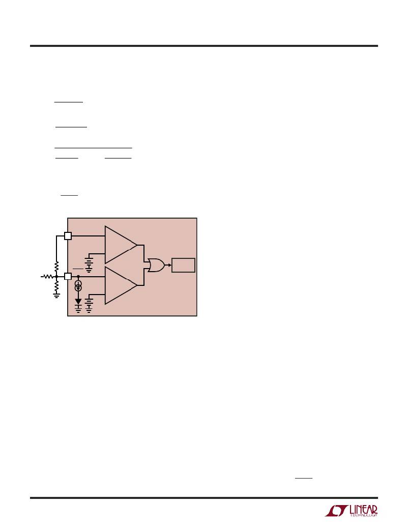
�Referring� to� Figure� 2,� the� PGFB� pin� is� the� positive� input� to�
�3434� F08�
�Figure� 8.� Undervoltage� Lockout�
�SYNCHRONIZING�
�Oscillator� synchronization� to� an� external� input� is� achieved�
�by� connecting� a� TTL� logic-compatible� square� wave� with� a�
�duty� cycle� between� 30%� and� 70%� to� the� LT3434� SYNC�
�pin.� The� synchronizing� range� is� equal� to� initial� operating�
�frequency� up� to� 700kHz.� This� means� that� minimum�
�practical� sync� frequency� is� equal� to� the� worst-case� high�
�self-oscillating� frequency� (230kHz),� not� the� typical� oper-�
�ating� frequency� of� 200kHz.� Caution� should� be� used� when�
�synchronizing� above� 230kHz� because� at� higher� sync�
�frequencies� the� amplitude� of� the� internal� slope� compen-�
�sation� used� to� prevent� subharmonic� switching� is� re-�
�duced.� This� type� of� subharmonic� switching� only� occurs� at�
�input� voltages� less� than� twice� output� voltage.� Higher�
�inductor� values� will� tend� to� eliminate� this� problem.� See�
�a� comparator� whose� negative� input� is� set� at� V� PGFB� .� When�
�PGFB� is� taken� above� V� PGFB� ,� current� (I� CSS� )� is� sourced� into�
�the� C� T� pin� starting� the� delay� period.� When� the� voltage� on�
�the� PGFB� pin� drops� below� V� PGFB� the� C� T� pin� is� rapidly�
�discharged� resetting� the� delay� period.� The� PGFB� voltage� is�
�typically� generated� by� a� resistive� divider� from� the� regu-�
�lated� output� or� input� supply.�
�The� capacitor� on� the� C� T� pin� determines� the� amount� of�
�delay� time� between� the� PGFB� pin� exceeding� its� threshold�
�(V� PGFB� )� and� the� PG� pin� set� to� a� high� impedance� state.�
�When� the� PGFB� pin� rises� above� V� PGFB� current� is� sourced�
�(I� CT� )� from� the� C� T� pin� into� the� external� capacitor.� When� the�
�voltage� on� the� external� capacitor� reaches� an� internal� clamp�
�(V� CT� ),� the� PG� pin� becomes� a� high� impedance� node.� The�
�resultant� PG� delay� time� is� given� by� t� =� C� CT� ?� (V� CT� )/(I� CT� ).� If�
�the� voltage� on� the� PGFB� pin� drops� below� its� V� PGFB� ,� C� CT� will�
�be� discharged� rapidly� and� PG� will� be� active� low� with� a�
�200� μ� A� sink� capability.� If� the� SHDN� pin� is� taken� below� its�
�3434fb�
�18�
�相关PDF资料 |
PDF描述 |
|---|---|
| LT3435IFE#PBF | IC REG BUCK ADJ 3A 16TSSOP |
| LT1370HVCT7 | IC REG MULTI CONFIG ADJ TO220-7 |
| LT1074IT | IC REG MULTI CONFIG ADJ TO220-5 |
| L04026R8BHLTR | INDUCTOR THIN FILM 6.8NH 0402 |
| L04025R6BHLTR | INDUCTOR THIN FILM 5.6NH 0402 |
相关代理商/技术参数 |
参数描述 |
|---|---|
| LT3434IFE#PBF | 功能描述:IC REG BUCK ADJ 3A 16TSSOP RoHS:是 类别:集成电路 (IC) >> PMIC - 稳压器 - DC DC 开关稳压器 系列:- 设计资源:Design Support Tool 标准包装:1 系列:- 类型:升压(升压) 输出类型:固定 输出数:1 输出电压:3V 输入电压:0.75 V ~ 2 V PWM 型:- 频率 - 开关:- 电流 - 输出:100mA 同步整流器:是 工作温度:-40°C ~ 85°C 安装类型:表面贴装 封装/外壳:SOT-23-5 细型,TSOT-23-5 包装:剪切带 (CT) 供应商设备封装:TSOT-23-5 其它名称:AS1323-BTTT-30CT |
| LT3434IFE#PBF | 制造商:Linear Technology 功能描述:IC, STEP-DOWN REGULATOR, 16-TSSOP |
| LT3434IFE#TR | 功能描述:IC REG BUCK ADJ 3A 16TSSOP RoHS:否 类别:集成电路 (IC) >> PMIC - 稳压器 - DC DC 开关稳压器 系列:- 设计资源:Design Support Tool 标准包装:1 系列:- 类型:升压(升压) 输出类型:固定 输出数:1 输出电压:3V 输入电压:0.75 V ~ 2 V PWM 型:- 频率 - 开关:- 电流 - 输出:100mA 同步整流器:是 工作温度:-40°C ~ 85°C 安装类型:表面贴装 封装/外壳:SOT-23-5 细型,TSOT-23-5 包装:剪切带 (CT) 供应商设备封装:TSOT-23-5 其它名称:AS1323-BTTT-30CT |
| LT3434IFE#TRPBF | 功能描述:IC REG BUCK ADJ 3A 16TSSOP RoHS:是 类别:集成电路 (IC) >> PMIC - 稳压器 - DC DC 开关稳压器 系列:- 设计资源:Design Support Tool 标准包装:1 系列:- 类型:升压(升压) 输出类型:固定 输出数:1 输出电压:3V 输入电压:0.75 V ~ 2 V PWM 型:- 频率 - 开关:- 电流 - 输出:100mA 同步整流器:是 工作温度:-40°C ~ 85°C 安装类型:表面贴装 封装/外壳:SOT-23-5 细型,TSOT-23-5 包装:剪切带 (CT) 供应商设备封装:TSOT-23-5 其它名称:AS1323-BTTT-30CT |
| LT3434IFEPBF | 制造商:Linear Technology 功能描述:DC-DC Converter Step-Down 60V TSSOP16EP |
发布紧急采购,3分钟左右您将得到回复。