- 您现在的位置:买卖IC网 > PDF目录13833 > LT3434IFE (Linear Technology)IC REG BUCK ADJ 3A 16TSSOP PDF资料下载
参数资料
| 型号: | LT3434IFE |
| 厂商: | Linear Technology |
| 文件页数: | 6/24页 |
| 文件大小: | 0K |
| 描述: | IC REG BUCK ADJ 3A 16TSSOP |
| 标准包装: | 95 |
| 类型: | 降压(降压) |
| 输出类型: | 可调式 |
| 输出数: | 1 |
| 输出电压: | 1.25 V ~ 54 V |
| 输入电压: | 3.3 V ~ 60 V |
| PWM 型: | 电流模式,混合 |
| 频率 - 开关: | 200kHz |
| 电流 - 输出: | 3A |
| 同步整流器: | 无 |
| 工作温度: | -40°C ~ 125°C |
| 安装类型: | 表面贴装 |
| 封装/外壳: | 16-TSSOP(0.173",4.40mm)裸露焊盘 |
| 包装: | 管件 |
| 供应商设备封装: | 16-TSSOP-EP |
�� �
�
�LT3434�
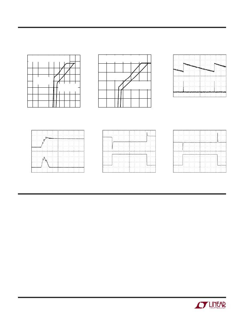
�TYPICAL� PERFOR� A� CE� CHARACTERISTICS�
�3.3V� Dropout� Operation�
�5V� Dropout� Operation�
�Burst� Mode� Operation�
�4.0�
�V� OUT� =� 3.3V�
�6�
�V� OUT� =� 5V�
�3.5�
�BOOST� DIODE� =� DIODES� INC� B1100�
�5�
�BOOST� DIODE� =� DIODES� INC� B1100�
�V� OUT�
�3.0�
�50mV/DIV�
�2.5�
�4�
�LOAD� CURRENT�
�2.0�
�1.5�
�1.0�
�0.5�
�0�
�LOAD� CURRENT�
�0.25A�
�LOAD� CURRENT�
�2.5A�
�3�
�2�
�1�
�0�
�0.25A�
�LOAD� CURRENT�
�2.5A�
�I� OUT�
�500mA/DIV�
�V� IN� =� 12V�
�V� OUT� =� 3.3V�
�I� Q� =� 100� μ� A�
�5ms/DIV�
�3434� G14�
�0�
�0.5�
�1�
�1.5�
�2�
�2.5�
�3�
�3.5�
�4�
�4.5�
�5�
�0�
�1�
�2�
�3�
�4�
�5�
�6�
�INPUT� VOLTAGE� (V)�
�3434� G24�
�INPUT� VOLTAGE� (V)�
�3434� G25�
�V� OUT�
�50mV/DIV�
�I� OUT�
�500mA/DIV�
�Burst� Mode� Operation�
�V� OUT�
�50mV/DIV�
�I� OUT�
�1A/DIV�
�No� Load� 2A� Step� Response�
�V� OUT�
�50mV/DIV�
�I� OUT�
�1A/DIV�
�Step� Response�
�V� IN� =� 12V�
�V� OUT� =� 3.3V�
�I� Q� =� 100� μ� A�
�5� μ� s/DIV�
�3434� G15�
�V� IN� =� 12V�
�V� OUT� =� 3.3V�
�C� OUT� =� 100� μ� F�
�500� μ� s/DIV�
�3434� G17�
�V� IN� = 12V 500μs/DIV�
�V� OUT� =� 3.3V�
�C� OUT� =� 100� μ� F�
�I� LOAD(DC)� =� 500mA�
�3434� G18�
�PI� FU� CTIO� S�
�NC� (Pin� 1):� No� Connection.�
�SW� (Pins� 2,� 5):� The� SW� pin� is� the� emitter� of� the� on-chip�
�power� NPN� switch.� This� pin� is� driven� up� to� the� input� pin�
�voltage� during� switch� on� time.� Inductor� current� drives� the�
�SW� pin� negative� during� switch� off� time.� Negative� voltage�
�is� clamped� with� the� external� catch� diode.� Maximum� nega-�
�tive� switch� voltage� allowed� is� –0.8V.�
�V� IN� (Pins� 3,� 4):� This� is� the� collector� of� the� on-chip� power�
�NPN� switch.� V� IN� powers� the� internal� control� circuitry� when�
�a� voltage� on� the� BIAS� pin� is� not� present.� High� dI/dt� edges�
�occur� on� this� pin� during� switch� turn� on� and� off.� Keep� the�
�path� short� from� the� V� IN� pin� through� the� input� bypass�
�capacitor,� through� the� catch� diode� back� to� SW.� All� trace�
�inductance� on� this� path� will� create� a� voltage� spike� at� switch�
�off,� adding� to� the� V� CE� voltage� across� the� internal� NPN.�
�BOOST� (Pin� 6):� The� BOOST� pin� is� used� to� provide� a� drive�
�voltage,� higher� than� the� input� voltage,� to� the� internal�
�bipolar� NPN� power� switch.� Without� this� added� voltage,� the�
�typical� switch� voltage� loss� would� be� about� 1.5V.� The�
�additional� BOOST� voltage� allows� the� switch� to� saturate�
�and� its� voltage� loss� approximates� that� of� a� 0.1� ?� FET�
�structure.�
�C� T� (Pin� 7):� A� capacitor� on� the� C� T� pin� determines� the� amount�
�of� delay� time� between� the� PGFB� pin� exceeding� its� thresh-�
�old� (V� PGFB� )� and� the� PG� pin� set� to� a� high� impedance� state.�
�When� the� PGFB� pin� rises� above� V� PGFB� ,� current� is� sourced�
�3434fb�
�6�
�相关PDF资料 |
PDF描述 |
|---|---|
| LT3435IFE#PBF | IC REG BUCK ADJ 3A 16TSSOP |
| LT1370HVCT7 | IC REG MULTI CONFIG ADJ TO220-7 |
| LT1074IT | IC REG MULTI CONFIG ADJ TO220-5 |
| L04026R8BHLTR | INDUCTOR THIN FILM 6.8NH 0402 |
| L04025R6BHLTR | INDUCTOR THIN FILM 5.6NH 0402 |
相关代理商/技术参数 |
参数描述 |
|---|---|
| LT3434IFE#PBF | 功能描述:IC REG BUCK ADJ 3A 16TSSOP RoHS:是 类别:集成电路 (IC) >> PMIC - 稳压器 - DC DC 开关稳压器 系列:- 设计资源:Design Support Tool 标准包装:1 系列:- 类型:升压(升压) 输出类型:固定 输出数:1 输出电压:3V 输入电压:0.75 V ~ 2 V PWM 型:- 频率 - 开关:- 电流 - 输出:100mA 同步整流器:是 工作温度:-40°C ~ 85°C 安装类型:表面贴装 封装/外壳:SOT-23-5 细型,TSOT-23-5 包装:剪切带 (CT) 供应商设备封装:TSOT-23-5 其它名称:AS1323-BTTT-30CT |
| LT3434IFE#PBF | 制造商:Linear Technology 功能描述:IC, STEP-DOWN REGULATOR, 16-TSSOP |
| LT3434IFE#TR | 功能描述:IC REG BUCK ADJ 3A 16TSSOP RoHS:否 类别:集成电路 (IC) >> PMIC - 稳压器 - DC DC 开关稳压器 系列:- 设计资源:Design Support Tool 标准包装:1 系列:- 类型:升压(升压) 输出类型:固定 输出数:1 输出电压:3V 输入电压:0.75 V ~ 2 V PWM 型:- 频率 - 开关:- 电流 - 输出:100mA 同步整流器:是 工作温度:-40°C ~ 85°C 安装类型:表面贴装 封装/外壳:SOT-23-5 细型,TSOT-23-5 包装:剪切带 (CT) 供应商设备封装:TSOT-23-5 其它名称:AS1323-BTTT-30CT |
| LT3434IFE#TRPBF | 功能描述:IC REG BUCK ADJ 3A 16TSSOP RoHS:是 类别:集成电路 (IC) >> PMIC - 稳压器 - DC DC 开关稳压器 系列:- 设计资源:Design Support Tool 标准包装:1 系列:- 类型:升压(升压) 输出类型:固定 输出数:1 输出电压:3V 输入电压:0.75 V ~ 2 V PWM 型:- 频率 - 开关:- 电流 - 输出:100mA 同步整流器:是 工作温度:-40°C ~ 85°C 安装类型:表面贴装 封装/外壳:SOT-23-5 细型,TSOT-23-5 包装:剪切带 (CT) 供应商设备封装:TSOT-23-5 其它名称:AS1323-BTTT-30CT |
| LT3434IFEPBF | 制造商:Linear Technology 功能描述:DC-DC Converter Step-Down 60V TSSOP16EP |
发布紧急采购,3分钟左右您将得到回复。