- 您现在的位置:买卖IC网 > PDF目录14810 > LT3439EFE#PBF (Linear Technology)IC REG PSH-PLL CTRLR ISO 16TSSOP PDF资料下载
参数资料
| 型号: | LT3439EFE#PBF |
| 厂商: | Linear Technology |
| 文件页数: | 8/12页 |
| 文件大小: | 0K |
| 描述: | IC REG PSH-PLL CTRLR ISO 16TSSOP |
| 标准包装: | 95 |
| 类型: | 推挽式控制器,隔离式 |
| 输出数: | 1 |
| 输入电压: | 2.8 V ~ 17.5 V |
| 频率 - 开关: | 20kHz ~ 250kHz |
| 电流 - 输出: | 1A |
| 同步整流器: | 无 |
| 工作温度: | -40°C ~ 125°C |
| 安装类型: | 表面贴装 |
| 封装/外壳: | 16-TSSOP(0.173",4.40mm)裸露焊盘 |
| 包装: | 管件 |
| 供应商设备封装: | 16-TSSOP-EP |
| 产品目录页面: | 1331 (CN2011-ZH PDF) |
�� �
�
�LT3439�
�APPLICATIO� S� I� FOR� ATIO�
�mean� greater� switching� losses� in� the� internal� output�
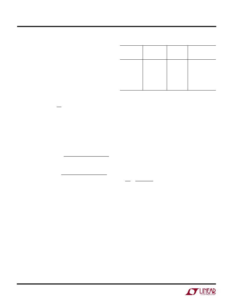
�Table� 1�
�switches.� However,� efficiency� is� only� modestly� reduced�
�NOMINAL�
�NOMINAL�
�for� a� large� improvement� in� EMI.�
�Care� should� be� taken� to� ensure� that� the� worst-case� input�
�voltage� and� load� current� conditions� do� not� cause� an�
�excessive� die� temperature.� The� total� power� dissipation� of�
�the� IC� is� dominated� by� three� loss� terms,� regulator� losses,�
�saturation� losses� and� switching� losses.� The� following�
�formulas� may� be� used� to� approximate� these� losses:�
�INPUT�
�VOLTAGE�
�5V�
�5V�
�5V�
�5V�
�5V�
�5V�
�12V�
�OUTPUT�
�VOLTAGE�
�12V�
�12V�
�±� 15V�
�±� 15V�
�12V�
�12V�
�–12V�
�OUTPUT�
�POWER�
�1.5W�
�3.0W�
�1.5W�
�3.0W�
�1.5W�
�10W�
�6W�
�COILTRONICS�
�PART� NUMBER�
�CTX02-13716-X1�
�CTX02-13665-X1�
�CTX02-13713-X1�
�CTX02-13664-X1�
�CTX02-13834-X3�
�CTX02-13949-X1�
�CTX02-16076�
�1.� Regulator� Dissipation:�
�These� transformers� will� yield� slightly� high� output� voltages�
�P� VIN� IN� ?� 12� mA� +�
�=� V�
�?�
�?�
�?�
�I� ?�
�60� ?�
�so� that� they� can� accommodate� an� LDO� regulator� on� the�
�output.�
�where� I� is� the� average� switch� current.�
�2.� Switch� Saturation� Dissipation:�
�P� VSAT� =� (V� SAT� )(I)�
�3.� Switch� Switching� Dissipation:�
�If� your� application� is� not� listed,� the� LTC� Applications� group�
�is� available� to� assist� in� the� choice� and/or� the� design� of� the�
�transformer.�
�In� the� design/selection� of� the� transformer� the� following�
�characteristics� are� critical� and� should� be� considered.�
�(�
�?� –� 2� .� 3� ?� 10�
�P� SW�
�=� 10� –� 6�
�?�
�?� V� IN� ?� I� ?� f� OSC� ?�
�?�
�I�
�–� 4� ?� R� SL� +� 10� .� 8�
�)�
�+�
�Turns� Ratio�
�The� turns� ratio� of� the� transformer� determines� the� output�
�voltage.� The� following� equation� can� be� used� as� a� first� pass�
�?�
�?�
�=� OUT� F�
�(�
�V�
�?�
�–� 1� .� 7� ?� 10� –� 3� ?� R� SL� +� 65� .� 8� )� ?�
�to� calculate� the� turns� ratio:�
�N� S� V� +� V�
�N� P� V� IN� –� V� SW�
�Total� IC� power� dissipation� (P� D� )� is� the� sum� of� these� three�
�terms.� Die� junction� temperature� can� be� computed� as�
�follows:�
�T� J� =� T� AMB� +� (P� D� )(� θ� JA� )�
�where� T� AMB� is� the� ambient� temperature,� T� J� is� the� junction�
�temperature� and� θ� JA� is� the� thermal� resistance� from� junc-�
�tion� to� ambient.�
�The� LT3439� comes� in� the� 16-pin� TSSOP� with� exposed�
�backside� package� that� has� a� very� low� junction-to-ambient�
�thermal� resistance� (� θ� JA� )� of� approximately� 40� °� C/W.�
�Transformer� Design�
�Table� 1� lists� recommended� center� tapped� transformers� for�
�a� variety� of� input� voltage,� output� voltage� and� power�
�combinations.�
�where� V� F� is� the� forward� voltage� of� the� output� diode� and�
�V� SW� is� the� voltage� drop� across� the� internal� switches� (see�
�Typical� Performance� curves).�
�Sufficient� margin� should� be� added� to� the� turns� ratio� to�
�account� for� voltage� drops� due� to� transformer� winding�
�resistances.� Also,� if� using� an� LDO� for� regulating� the� output�
�voltage,� don’t� forget� to� take� into� account� the� voltage� drop�
�that� should� be� added� to� V� OUT� .�
�Magnetizing� Current�
�The� primary� inductance� of� the� transformer� causes� a� ripple�
�current� that� is� independent� of� load� current.� The� ripple�
�current� manifests� itself� in� the� output� voltage� through� the�
�parasitic� resistances� of� the� supply.� Increasing� the� trans-�
�former� magnetizing� inductance� can� reduce� the� ripple�
�sn3439� 3439fs�
�8�
�相关PDF资料 |
PDF描述 |
|---|---|
| RCM31DRMH | CONN EDGECARD 62POS .156 WW |
| LTC3428EDD#PBF | IC REG BOOST ADJ 4A 10DFN |
| LTC3421EUF#PBF | IC REG BOOST SYNC ADJ 1.5A 24QFN |
| LT3501EFE#PBF | IC REG BUCK ADJ 3A DL 20TSSOP |
| LT3508EFE#PBF | IC REG BUCK ADJ 1.4A DL 16TSSOP |
相关代理商/技术参数 |
参数描述 |
|---|---|
| LT343L | 制造商:未知厂家 制造商全称:未知厂家 功能描述:Optoelectronic |
| LT344L | 制造商:未知厂家 制造商全称:未知厂家 功能描述:Optoelectronic |
| LT344LR | 制造商:未知厂家 制造商全称:未知厂家 功能描述:Optoelectronic |
| LT3460 | 制造商:LINER 制造商全称:Linear Technology 功能描述:1.3MHz Step-Up DC/DC Converter in SC70 and ThinSOT |
| LT3460EDC-1#PBF | 制造商:Linear Technology 功能描述:SP-SWREG/Monolithic, CUT TAPE 150mA, 650kHz Boost Converter in 2x2 DFN |
发布紧急采购,3分钟左右您将得到回复。