- 您现在的位置:买卖IC网 > PDF目录14797 > LT3506AIDHD#PBF (Linear Technology)IC REG BUCK ADJ 1.6A DL 16DFN PDF资料下载
参数资料
| 型号: | LT3506AIDHD#PBF |
| 厂商: | Linear Technology |
| 文件页数: | 12/24页 |
| 文件大小: | 0K |
| 描述: | IC REG BUCK ADJ 1.6A DL 16DFN |
| 标准包装: | 73 |
| 类型: | 降压(降压) |
| 输出类型: | 可调式 |
| 输出数: | 2 |
| 输出电压: | 0.8 V ~ 22 V |
| 输入电压: | 3.6 V ~ 25 V |
| PWM 型: | 电流模式 |
| 频率 - 开关: | 1.1MHz |
| 电流 - 输出: | 1.6A |
| 同步整流器: | 无 |
| 工作温度: | -40°C ~ 125°C |
| 安装类型: | 表面贴装 |
| 封装/外壳: | 16-WFDFN 裸露焊盘 |
| 包装: | 管件 |
| 供应商设备封装: | 16-DFN(5x4) |
| 产品目录页面: | 1331 (CN2011-ZH PDF) |
�� �
�
�LT3506/LT3506A�
�APPLICATIONS� INFORMATION�
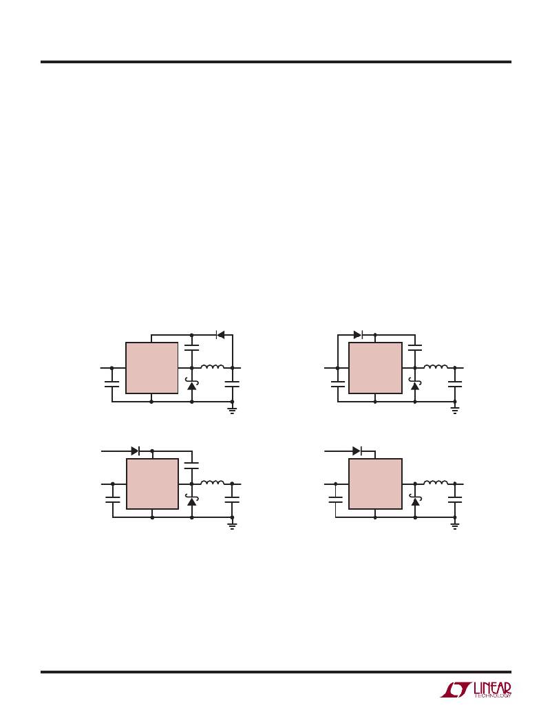
�BOOST� Pin� Considerations�
�The� capacitor� and� diode� tied� to� the� BOOST� pin� generate�
�a� voltage� that� is� higher� than� the� input� voltage.� In� most�
�cases� a� 0.1μF� capacitor� and� fast� switching� diode� (such�
�as� the� CMDSH-3� or� FMMD914)� will� work� well.� Figure� 3�
�shows� three� ways� to� arrange� the� boost� circuit.� The� BOOST�
�pin� must� be� more� than� 2.5V� above� the� SW� pin� for� full�
�ef?ciency.� For� outputs� of� 3.3V� and� higher� the� standard�
�circuit� (Figure� 3a)� is� best.� For� outputs� between� 2.8V� and�
�3.3V,� use� a� small� Schottky� diode� (such� as� the� BAT-54).�
�For� lower� output� voltages� the� boost� diode� can� be� tied� to�
�the� input� (Figure� 3b).� The� circuit� in� Figure� 3a� is� more� ef-�
�?cient� because� the� BOOST� pin� current� comes� from� a� lower�
�voltage� source.� Finally,� as� shown� in� Figure� 3c,� the� anode�
�of� the� boost� diode� can� be� tied� to� another� source� that� is�
�at� least� 3V.� For� example,� if� you� are� generating� 3.3V� and�
�D2�
�1.8V� and� the� 3.3V� is� on� whenever� the� 1.8V� is� on,� the� 1.8V�
�boost� diode� can� be� connected� to� the� 3.3V� output.� In� any�
�case,� you� must� also� be� sure� that� the� maximum� voltage� at�
�the� BOOST� pin� is� less� than� the� maximum� speci?ed� in� the�
�Absolute� Maximum� Ratings� section.�
�The� boost� circuit� can� also� run� directly� from� a� DC� voltage�
�that� is� higher� than� the� input� voltage� by� more� than� 3V,�
�as� in� Figure� 3d.� The� diode� is� used� to� prevent� damage� to�
�the� LT3506� in� case� V� INB� is� held� low� while� V� IN� is� present.�
�The� circuit� saves� several� components� (both� BOOST� pins�
�can� be� tied� to� D2).� However,� ef?ciency� may� be� lower� and�
�dissipation� in� the� LT3506� may� be� higher.� Also,� if� V� INB� is�
�absent,� the� LT3506� will� still� attempt� to� regulate� the� output,�
�but� will� do� so� with� very� low� ef?ciency� and� high� dissipation�
�because� the� switch� will� not� be� able� to� saturate,� dropping�
�1.5V� to� 2V� in� conduction.�
�D2�
�BOOST�
�LT3506�
�C3�
�BOOST�
�LT3506�
�C3�
�V� IN�
�V� IN�
�SW�
�V� OUT�
�V� IN�
�V� IN�
�SW�
�V� OUT�
�GND�
�GND�
�V� BOOST� –� V� SW�
�MAX� V� BOOST�
�V� OUT�
�V� IN� +� V� OUT�
�(3a)�
�V� BOOST� –� V� SW�
�MAX� V� BOOST�
�V� IN�
�2V� IN�
�(3b)�
�V� INB� >� 3V�
�D2�
�BOOST�
�LT3506�
�C3�
�V� INB�
�>V� IN� +� 3V�
�D2�
�BOOST�
�LT3506�
�V� IN�
�V� IN�
�SW�
�V� OUT�
�V� IN�
�V� IN�
�SW�
�V� OUT�
�GND�
�GND�
�V� BOOST� –� V� SW�
�MAX� V� BOOST�
�V� INB�
�V� INB� +� V� IN�
�MAX� V� BOOST� –� V� SW�
�MAX� V� BOOST�
�V� INB�
�V� INB�
�3506� F03�
�MINIMUM� VALUE� FOR� V� INB� =� 3V�
�(3c)�
�MINIMUM� VALUE� FOR� V� INB� =� V� IN� +� 3V�
�(3d)�
�Figure� 3.� Generating� the� Boost� Voltage�
�3506afc�
�12�
�相关PDF资料 |
PDF描述 |
|---|---|
| 9230-94-RC | CHOKE RF MOLDED .1UH 10%PHENOLIC |
| LTC3603EUF#PBF | IC REG BUCK SYNC ADJ 2.5A 20QFN |
| 1140-2R2M | CHOKE RF RADIAL 2.2UH 20% |
| LGU1K182MELB | CAP ALUM 1800UF 80V 20% SNAP |
| LGU2P471MELB | CAP ALUM 470UF 220V 20% SNAP |
相关代理商/技术参数 |
参数描述 |
|---|---|
| LT3506AIDHD-TR | 制造商:LINER 制造商全称:Linear Technology 功能描述:Dual Monolithic 1.6A Step-Down Switching Regulator |
| LT3506AIDHD-TRPBF | 制造商:LINER 制造商全称:Linear Technology 功能描述:Dual Monolithic 1.6A Step-Down Switching Regulator |
| LT3506AIFE | 制造商:LINER 制造商全称:Linear Technology 功能描述:Dual Monolithic 1.6A Step-Down Switching Regulator |
| LT3506AIFE#PBF | 功能描述:IC REG BUCK ADJ 1.6A DL 16TSSOP RoHS:是 类别:集成电路 (IC) >> PMIC - 稳压器 - DC DC 开关稳压器 系列:- 设计资源:Design Support Tool 标准包装:1 系列:- 类型:升压(升压) 输出类型:固定 输出数:1 输出电压:3V 输入电压:0.75 V ~ 2 V PWM 型:- 频率 - 开关:- 电流 - 输出:100mA 同步整流器:是 工作温度:-40°C ~ 85°C 安装类型:表面贴装 封装/外壳:SOT-23-5 细型,TSOT-23-5 包装:剪切带 (CT) 供应商设备封装:TSOT-23-5 其它名称:AS1323-BTTT-30CT |
| LT3506AIFE#TRPBF | 功能描述:IC REG BUCK ADJ 1.6A DL 16TSSOP RoHS:是 类别:集成电路 (IC) >> PMIC - 稳压器 - DC DC 开关稳压器 系列:- 设计资源:Design Support Tool 标准包装:1 系列:- 类型:升压(升压) 输出类型:固定 输出数:1 输出电压:3V 输入电压:0.75 V ~ 2 V PWM 型:- 频率 - 开关:- 电流 - 输出:100mA 同步整流器:是 工作温度:-40°C ~ 85°C 安装类型:表面贴装 封装/外壳:SOT-23-5 细型,TSOT-23-5 包装:剪切带 (CT) 供应商设备封装:TSOT-23-5 其它名称:AS1323-BTTT-30CT |
发布紧急采购,3分钟左右您将得到回复。