- 您现在的位置:买卖IC网 > PDF目录44984 > LT3509IMSE#TRPBF (LINEAR TECHNOLOGY CORP) 1.2 A DUAL SWITCHING CONTROLLER, 2500 kHz SWITCHING FREQ-MAX, PDSO16 PDF资料下载
参数资料
| 型号: | LT3509IMSE#TRPBF |
| 厂商: | LINEAR TECHNOLOGY CORP |
| 元件分类: | 稳压器 |
| 英文描述: | 1.2 A DUAL SWITCHING CONTROLLER, 2500 kHz SWITCHING FREQ-MAX, PDSO16 |
| 封装: | LEAD FREE, PLASTIC, MSOP-16 |
| 文件页数: | 11/24页 |
| 文件大小: | 271K |
| 代理商: | LT3509IMSE#TRPBF |
LT3509
19
3509fc
APPLICATIONS INFORMATION
Hot Plugging Considerations
The small size, reliability and low impedance of ceramic
capacitors make them attractive for the input capacitor.
Unfortunately they can be hazardous to semiconductor
devices if combined with an inductive supply loop and a
fast power transition such as through a mechanical switch
or connector. The low loss ceramic capacitor combined
with the just a small amount of wiring inductance forms
an underdamped resonant tank circuit and the voltage at
the VIN pin of the LT3509 can ring to twice the nominal
input voltage. See Linear Technology Application Note 88
for more details.
PCB Layout and Thermal Design
The PCB layout is critical to both the electrical and thermal
performance of the LT3509. Most important is the connec-
tion to the Exposed Pad which provides the main ground
connection and also a thermal path for cooling the chip.
This must be soldered to a topside copper plane which
is also tied to backside and/or internal plane(s) with an
array of thermal vias.
To obtain the best electrical performance particular
attention should be paid to keeping the following current
paths short:
The loop from the VIN pin through the input capacitor
back to the ground pad and plane. This sees high di/dt
transitions as the power switches turn on and off. Ex-
cess impedance will degrade the minimum usable input
voltage and could cause crosstalk between channels.
The loops from the switch pins to the catch diodes and
back to the DA pins. The fast changing currents and
voltage here combined with long PCB traces will cause
ringing on the switch pin and may result in unwelcome
EMI.
The loop from the regulated outputs through the output
capacitor back to the ground plane. Excess impedance
here will result in excessive ripple at the output.
The area of the SW and BOOST nodes should as small as
possible. Also the feedback components should be placed
as close as possible to the FB pins so that the traces are
short and shielded from the SW and BOOST nodes by the
ground planes.
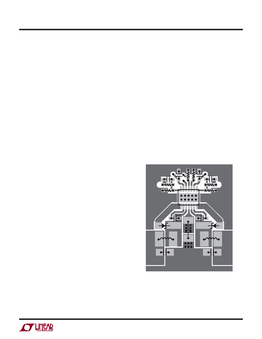
Figure 13 shows a detail view of a practical board layout
showing just the top layer. The complete board is somewhat
larger at 7.5cm × 7.5cm. The device has been evaluated
on this board in still air running at 700kHz switching fre-
quency. One channel was set to 5V and the other to 3.3V
and both channels were fully loaded to 700mA. The device
temperature reached approximately 15°C above ambient
for input voltages below 12V. At 24V input it was slightly
higher at 17°C above ambient.
Figure 13. Sample PCB Layout (Top Layer Only)
相关PDF资料 |
PDF描述 |
|---|---|
| LT3509EMSE#TRPBF | 1.2 A DUAL SWITCHING CONTROLLER, 2500 kHz SWITCHING FREQ-MAX, PDSO16 |
| LT3509IDE#TRPBF | 1.2 A DUAL SWITCHING CONTROLLER, 2500 kHz SWITCHING FREQ-MAX, PDSO14 |
| LT3509IDE#PBF | 1.2 A DUAL SWITCHING CONTROLLER, 2500 kHz SWITCHING FREQ-MAX, PDSO14 |
| LT3509EDE#PBF | 1.2 A DUAL SWITCHING CONTROLLER, 2500 kHz SWITCHING FREQ-MAX, PDSO14 |
| LT3509EDE#TRPBF | 1.2 A DUAL SWITCHING CONTROLLER, 2500 kHz SWITCHING FREQ-MAX, PDSO14 |
相关代理商/技术参数 |
参数描述 |
|---|---|
| LT350A | 功能描述:气体放电管 - GDT /气体等离子体避雷器 350V RoHS:否 制造商:Bourns 峰值脉冲电流: 直流击穿电压(标称):4500 V 电极数量:2 系列:SA2 端接类型:Axial 故障安全保护 Y/N: 封装:Reel |
| LT350A-B | 功能描述:气体放电管 - GDT /气体等离子体避雷器 350V RoHS:否 制造商:Bourns 峰值脉冲电流: 直流击穿电压(标称):4500 V 电极数量:2 系列:SA2 端接类型:Axial 故障安全保护 Y/N: 封装:Reel |
| LT350AK | 制造商:Linear Technology 功能描述:Standard Regulator Pos 3A 3-Pin(2+Tab) TO-3 |
| LT350AT | 制造商:未知厂家 制造商全称:未知厂家 功能描述:Positive Adjustable Voltage Regulator |
| LT350C | 功能描述:气体放电管 - GDT /气体等离子体避雷器 350V RoHS:否 制造商:Bourns 峰值脉冲电流: 直流击穿电压(标称):4500 V 电极数量:2 系列:SA2 端接类型:Axial 故障安全保护 Y/N: 封装:Reel |
发布紧急采购,3分钟左右您将得到回复。