- 您现在的位置:买卖IC网 > PDF目录44984 > LT3509IMSE#TRPBF (LINEAR TECHNOLOGY CORP) 1.2 A DUAL SWITCHING CONTROLLER, 2500 kHz SWITCHING FREQ-MAX, PDSO16 PDF资料下载
参数资料
| 型号: | LT3509IMSE#TRPBF |
| 厂商: | LINEAR TECHNOLOGY CORP |
| 元件分类: | 稳压器 |
| 英文描述: | 1.2 A DUAL SWITCHING CONTROLLER, 2500 kHz SWITCHING FREQ-MAX, PDSO16 |
| 封装: | LEAD FREE, PLASTIC, MSOP-16 |
| 文件页数: | 4/24页 |
| 文件大小: | 271K |
| 代理商: | LT3509IMSE#TRPBF |
LT3509
12
3509fc
APPLICATIONS INFORMATION
Minimum Input Voltage and Boost Architecture
The minimum operating voltage is determined either by
the LT3509’s internal undervoltage lockout of ~3.6V or
by its maximum duty cycle. The maximum duty cycle for
xed frequency operation is given by:
DC
t
f
MAX
OFF MIN
SW
=
1
()
It follows that:
V
VV
DC
VV
IN MIN
OUT
F
MAX
FSW
() =
+
+
If a reduction in switching frequency can be tolerated the
minimum input voltage can drop to just above output
voltage. Not only is the output transistor base pumped
above the input voltage by the boost capacitor, the
switch can remain on through multiple switching cycles
resulting in a high effective duty cycle. Thus, this is a
true low dropout regulator. As it is necessary to recharge
the boost capacitor from time to time, a minimum width
off-cycle will be forced occasionally to maintain the charge.
Depending on the operating frequency, the duty cycle can
reach 97% to 98%, although at this point the output pulses
will be at a sub-multiple of the programmed frequency.
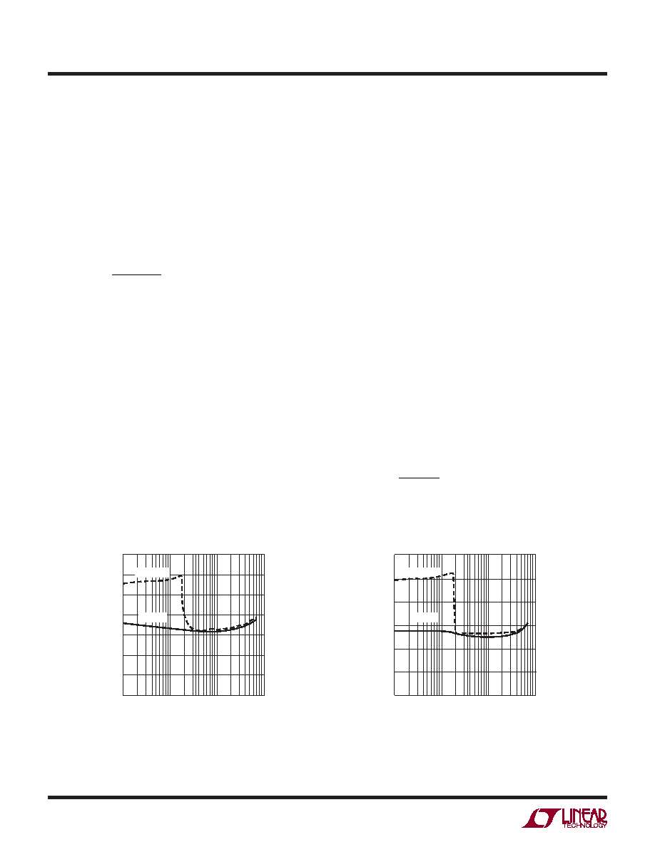
One other consideration is that at very light loads or no
load the part will go into pulse skipping mode. The part
will then have trouble getting enough voltage on to the
boost capacitors to fully saturate the switch. This is most
problematic when the BD pin is supplied from the regulated
output. The net result is that a higher input voltage will be
required to start up the boost system. The typical minimum
input voltage over a range of loads is shown in Figure 5
for 3.3V and Figure 6 for 5V.
When operating at such high duty cycles the peak currents
in the boost diodes are greater and this will require a the
BD supply to be somewhat higher than would be required
at less extreme duty cycles. If operation at low input/output
ratios and low BD supply voltages is required it may be
desirable to augment the internal boost diodes with external
discrete diodes in parallel.
Boost Pin Considerations
The boost capacitor, in conjunction with the internal boost
diode, provides a bootstrapped supply for the power switch
that is above the input voltage. For operation at 1MHz and
above and at reasonable duty cycles a 0.1μF capacitor
will work well. For operation at lower frequencies and/or
higher duty cycles something larger may be needed. A
good rule of thumb is:
C
f
BOOST
SW
=
1
10
where fSW is in MHz and CBOOST is in μF
Figure 5. Minimum VIN for 3.3V VOUT
LOAD CURRENT (A)
0.001
V
IN
TO
ST
AR
T
(V)
4
4.5
5
1
3509 F05
3
3.5
2.5
2
0.01
0.1
5.5
TO START
TO RUN
Figure 6. Minimum VIN for 5V VOUT
LOAD CURRENT (A)
0.001
V
IN
TO
ST
AR
T
(V)
6
6.5
1
3509 F06
5
5.5
4.5
4
0.01
0.1
7
TO START
TO RUN
相关PDF资料 |
PDF描述 |
|---|---|
| LT3509EMSE#TRPBF | 1.2 A DUAL SWITCHING CONTROLLER, 2500 kHz SWITCHING FREQ-MAX, PDSO16 |
| LT3509IDE#TRPBF | 1.2 A DUAL SWITCHING CONTROLLER, 2500 kHz SWITCHING FREQ-MAX, PDSO14 |
| LT3509IDE#PBF | 1.2 A DUAL SWITCHING CONTROLLER, 2500 kHz SWITCHING FREQ-MAX, PDSO14 |
| LT3509EDE#PBF | 1.2 A DUAL SWITCHING CONTROLLER, 2500 kHz SWITCHING FREQ-MAX, PDSO14 |
| LT3509EDE#TRPBF | 1.2 A DUAL SWITCHING CONTROLLER, 2500 kHz SWITCHING FREQ-MAX, PDSO14 |
相关代理商/技术参数 |
参数描述 |
|---|---|
| LT350A | 功能描述:气体放电管 - GDT /气体等离子体避雷器 350V RoHS:否 制造商:Bourns 峰值脉冲电流: 直流击穿电压(标称):4500 V 电极数量:2 系列:SA2 端接类型:Axial 故障安全保护 Y/N: 封装:Reel |
| LT350A-B | 功能描述:气体放电管 - GDT /气体等离子体避雷器 350V RoHS:否 制造商:Bourns 峰值脉冲电流: 直流击穿电压(标称):4500 V 电极数量:2 系列:SA2 端接类型:Axial 故障安全保护 Y/N: 封装:Reel |
| LT350AK | 制造商:Linear Technology 功能描述:Standard Regulator Pos 3A 3-Pin(2+Tab) TO-3 |
| LT350AT | 制造商:未知厂家 制造商全称:未知厂家 功能描述:Positive Adjustable Voltage Regulator |
| LT350C | 功能描述:气体放电管 - GDT /气体等离子体避雷器 350V RoHS:否 制造商:Bourns 峰值脉冲电流: 直流击穿电压(标称):4500 V 电极数量:2 系列:SA2 端接类型:Axial 故障安全保护 Y/N: 封装:Reel |
发布紧急采购,3分钟左右您将得到回复。