参数资料
| 型号: | LT3510IFE#TRPBF |
| 厂商: | Linear Technology |
| 文件页数: | 17/30页 |
| 文件大小: | 0K |
| 描述: | IC REG BUCK ADJ 2A DL 20TSSOP |
| 标准包装: | 2,500 |
| 类型: | 降压(降压) |
| 输出类型: | 可调式 |
| 输出数: | 2 |
| 输出电压: | 0.8 V ~ 23.8 V |
| 输入电压: | 3.1 V ~ 25 V |
| PWM 型: | 电流模式 |
| 频率 - 开关: | 250kHz ~ 1.5MHz |
| 电流 - 输出: | 2A |
| 同步整流器: | 无 |
| 工作温度: | -40°C ~ 125°C |
| 安装类型: | 表面贴装 |
| 封装/外壳: | 20-TSSOP(0.173",4.40mm 宽)裸露焊盘 |
| 包装: | 带卷 (TR) |
| 供应商设备封装: | 20-TSSOP-EP |
第1页第2页第3页第4页第5页第6页第7页第8页第9页第10页第11页第12页第13页第14页第15页第16页当前第17页第18页第19页第20页第21页第22页第23页第24页第25页第26页第27页第28页第29页第30页
�� �
�
�LT3510�
�APPLICATIONS� INFORMATION�
�Table� 2�
�where� I� OUT(MAX)� is� the� maximum� load� current,� and�
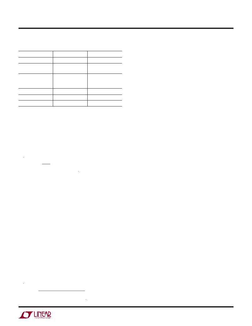
�VENDOR�
�Taiyo� Yuden�
�AVX�
�Kemet�
�Sanyo�
�Panasonic�
�TDK�
�TYPE�
�Ceramic� X5R,� X7R�
�Ceramic� X5R,� X7R�
�Tantalum�
�Tantalum�
�TA� Organic�
�AL� Organic�
�TA/AL� Organic�
�AL� Organic�
�Ceramic� X5R,� X7R�
�SERIES�
�T491,� T494,� T495�
�T520�
�A700�
�POSCAP�
�SP� CAP�
�V� BST(MIN)� is� the� minimum� boost� voltage� to� fully� saturate�
�the� switch.�
�Figure� 5� shows� four� ways� to� arrange� the� boost� circuit.� The�
�BST� pin� must� be� more� than� 1.4V� above� the� SW� pin� for�
�full� ef?ciency.� Generally,� for� outputs� of� 3.3V� and� higher�
�the� standard� circuit� (Figure� 5a)� is� the� best.� For� outputs�
�between� 2.8V� and� 3.3V,� replace� the� D2� with� a� small� Schottky�
�diode� such� as� the� PMEG4005.� For� lower� output� voltages�
�the� boost� diode� can� be� tied� to� the� input� (Figure� 5b).� The�
�circuit� in� Figure� 5a� is� more� ef?cient� because� the� BST�
�Catch� Diode�
�The� diode� D1� conducts� current� only� during� switch� off�
�time.� Use� a� Schottky� diode� to� limit� forward� voltage� drop� to�
�increase� ef?ciency.� The� Schottky� diode� must� have� a� peak�
�reverse� voltage� that� is� equal� to� regulator� input� voltage� and�
�sized� for� average� forward� current� in� normal� operation.�
�Average� forward� current� can� be� calculated� from:�
�pin� current� comes� from� a� lower� voltage� source.� Figure�
�5c� shows� the� boost� voltage� source� from� available� DC�
�sources� that� are� greater� than� 3V.� The� highest� ef?ciency� is�
�attained� by� choosing� the� lowest� boost� voltage� above� 3V.�
�For� example,� if� you� are� generating� 3.3V� and� 1.8V� and� the�
�3.3V� is� on� whenever� the� 1.8V� is� on,� the� 1.8V� boost� diode�
�can� be� connected� to� the� 3.3V� output.� In� any� case,� you�
�must� also� be� sure� that� the� maximum� voltage� at� the� BST�
�I� D(AVG)� =�
�I� OUT�
�V� IN�
�?� (� V� IN� –� V� OUT� )�
�pin� is� less� than� the� maximum� speci?ed� in� the� Absolute�
�Maximum� Ratings� section.�
�The� only� reason� to� consider� a� larger� diode� is� the� worst-�
�case� condition� of� a� high� input� voltage� and� shorted� output.�
�With� a� shorted� condition,� diode� current� will� increase� to� a�
�typical� value� of� 3A,� determined� by� the� peak� switch� current�
�limit� of� the� LT3510.� This� is� safe� for� short� periods� of� time,�
�but� it� would� be� prudent� to� check� with� the� diode� manu-�
�facturer� if� continuous� operation� under� these� conditions�
�can� be� tolerated.�
�BST� Pin� Considerations�
�The� capacitor� and� diode� tied� to� the� BST� pin� generate�
�a� voltage� that� is� higher� than� the� input� voltage.� In� most�
�cases� a� 0.47μF� capacitor� and� fast� switching� diode� (such�
�as� the� CMDSH-3� or� FMMD914)� will� work� well.� Almost�
�any� type� of� ?lm� or� ceramic� capacitor� is� suitable,� but� the�
�ESR� should� be� <1� Ω� to� ensure� it� can� be� fully� recharged�
�during� the� off� time� of� the� switch.� The� capacitor� value� can�
�be� approximated� by:�
�The� boost� circuit� can� also� run� directly� from� a� DC� voltage�
�that� is� higher� than� the� input� voltage� by� more� than� 3V,� as�
�in� Figure� 5d.� The� diode� is� used� to� prevent� damage� to� the�
�LT3510� in� case� V� X� is� held� low� while� V� IN� is� present.� The�
�circuit� saves� several� components� (both� BST� pins� can� be�
�tied� to� D2).� However,� ef?ciency� may� be� lower� and� dissipa-�
�tion� in� the� LT3510� may� be� higher.� Also,� if� V� X� is� absent,� the�
�LT3510� will� still� attempt� to� regulate� the� output,� but� will� do�
�so� with� very� low� ef?ciency� and� high� dissipation� because�
�the� switch� will� not� be� able� to� saturate,� dropping� 1.5V� to�
�2V� in� conduction.�
�The� minimum� input� voltage� of� an� LT3510� application� is�
�limited� by� the� minimum� operating� voltage� (<3V)� and� by�
�the� maximum� duty� cycle� as� outlined� above.� For� proper�
�start-up,� the� minimum� input� voltage� is� also� limited� by�
�the� boost� circuit.� If� the� input� voltage� is� ramped� slowly,� or�
�the� LT3510� is� turned� on� with� its� SS� pin� when� the� output�
�is� already� in� regulation,� then� the� boost� capacitor� may� not�
�be� fully� charged.� Because� the� boost� capacitor� is� charged�
�C� BST� =�
�B� ?� (� V� OUT� –� V� BST(MIN)� )� ?� f�
�I� OUT(MAX)� ?� DC�
�with� the� energy� stored� in� the� inductor,� the� circuit� will� rely�
�on� some� minimum� load� current� to� get� the� boost� circuit�
�running� properly.� This� minimum� load� will� depend� on�
�3510fe�
�17�
�相关PDF资料 |
PDF描述 |
|---|---|
| LT3511MPMS#PBF | IC REG FLYBK ISO ADJ .24A 16MSOP |
| LT3512MPMS#TRPBF | IC REG FLYBK ISO ADJ .42A 16MSOP |
| LT3513IUHF#PBF | IC REG 5-OUT FOR TFT-LCD 38QFN |
| LT3571IUD#TRPBF | IC REG BOOST ADJ 0.47A 16QFN |
| LT3573IMSE#TRPBF | IC REG FLYBACK ISO ADJ 16MSOP |
相关代理商/技术参数 |
参数描述 |
|---|---|
| LT3511 | 制造商:LINER 制造商全称:Linear Technology 功能描述:Monolithic High Voltage Isolated Flyback Converter No External Start-Up Resistor |
| LT3511EMS#PBF | 功能描述:IC REG FLYBACK ISOLATD 16-MSOP RoHS:是 类别:集成电路 (IC) >> PMIC - 稳压器 - DC DC 开关稳压器 系列:- 标准包装:250 系列:- 类型:降压(降压) 输出类型:固定 输出数:1 输出电压:1.2V 输入电压:2.05 V ~ 6 V PWM 型:电压模式 频率 - 开关:2MHz 电流 - 输出:500mA 同步整流器:是 工作温度:-40°C ~ 85°C 安装类型:表面贴装 封装/外壳:6-UFDFN 包装:带卷 (TR) 供应商设备封装:6-SON(1.45x1) 产品目录页面:1032 (CN2011-ZH PDF) 其它名称:296-25628-2 |
| LT3511EMS#TRPBF | 功能描述:IC REG FLYBK ISO ADJ .24A 16MSOP RoHS:是 类别:集成电路 (IC) >> PMIC - 稳压器 - DC DC 开关稳压器 系列:- 标准包装:2,500 系列:- 类型:降压(降压) 输出类型:固定 输出数:1 输出电压:1.2V,1.5V,1.8V,2.5V 输入电压:2.7 V ~ 20 V PWM 型:- 频率 - 开关:- 电流 - 输出:50mA 同步整流器:是 工作温度:-40°C ~ 125°C 安装类型:表面贴装 封装/外壳:10-TFSOP,10-MSOP(0.118",3.00mm 宽)裸露焊盘 包装:带卷 (TR) 供应商设备封装:10-MSOP 裸露焊盘 |
| LT3511HMS#PBF | 功能描述:IC REG FLYBK ISO ADJ .24A 16MSOP RoHS:是 类别:集成电路 (IC) >> PMIC - 稳压器 - DC DC 开关稳压器 系列:- 设计资源:Design Support Tool 标准包装:1 系列:- 类型:升压(升压) 输出类型:固定 输出数:1 输出电压:3V 输入电压:0.75 V ~ 2 V PWM 型:- 频率 - 开关:- 电流 - 输出:100mA 同步整流器:是 工作温度:-40°C ~ 85°C 安装类型:表面贴装 封装/外壳:SOT-23-5 细型,TSOT-23-5 包装:剪切带 (CT) 供应商设备封装:TSOT-23-5 其它名称:AS1323-BTTT-30CT |
| LT3511HMS#TRPBF | 功能描述:IC REG FLYBK ISO ADJ .24A 16MSOP RoHS:是 类别:集成电路 (IC) >> PMIC - 稳压器 - DC DC 开关稳压器 系列:- 设计资源:Design Support Tool 标准包装:1 系列:- 类型:升压(升压) 输出类型:固定 输出数:1 输出电压:3V 输入电压:0.75 V ~ 2 V PWM 型:- 频率 - 开关:- 电流 - 输出:100mA 同步整流器:是 工作温度:-40°C ~ 85°C 安装类型:表面贴装 封装/外壳:SOT-23-5 细型,TSOT-23-5 包装:剪切带 (CT) 供应商设备封装:TSOT-23-5 其它名称:AS1323-BTTT-30CT |
发布紧急采购,3分钟左右您将得到回复。